Imaging device and image processing method

a technology of imaging device and image processing method, which is applied in the direction of color television details, television systems, instruments, etc., can solve the problems of difficult manufacturing of lightweight and small-sized imaging devices, increasing the number of lenses that are driven in the cylindrical barrel to the extent that a much greater driving torque is required, and achieving constant angle of view

Inactive Publication Date: 2010-01-26
SAMSUNG ELECTRONICS CO LTD
View PDF9 Cites 7 Cited by
  • Summary
  • Abstract
  • Description
  • Claims
  • Application Information

AI Technical Summary

Benefits of technology

[0008]The present invention provides a small-sized and light weight imaging device and an image processing method that are capable of maintaining a constant angle of view even when a focal distance of an entire lens system changes depending on movements of a focusing lens.

Problems solved by technology

In imaging devices such as still cameras there has been a problem in that when focusing is performed at a very long or short distance by a focusing lens of a lens optical system, an angle of view changes in order to vary a focal distance of an entire lens system.
However, as disclosed in Japanese Patent No. 2503442, a cylindrical barrel containing a lens is large and the number of lenses that are driven in the cylindrical barrel increases to the extent that a much greater driving torque is required.
Therefore, it is difficult to manufacture a lightweight and small-sized imaging device that maintains a constant angle of view.

Method used


Image

  • Imaging device and image processing method
  • Imaging device and image processing method
  • Imaging device and image processing method

Examples


Embodiment Construction

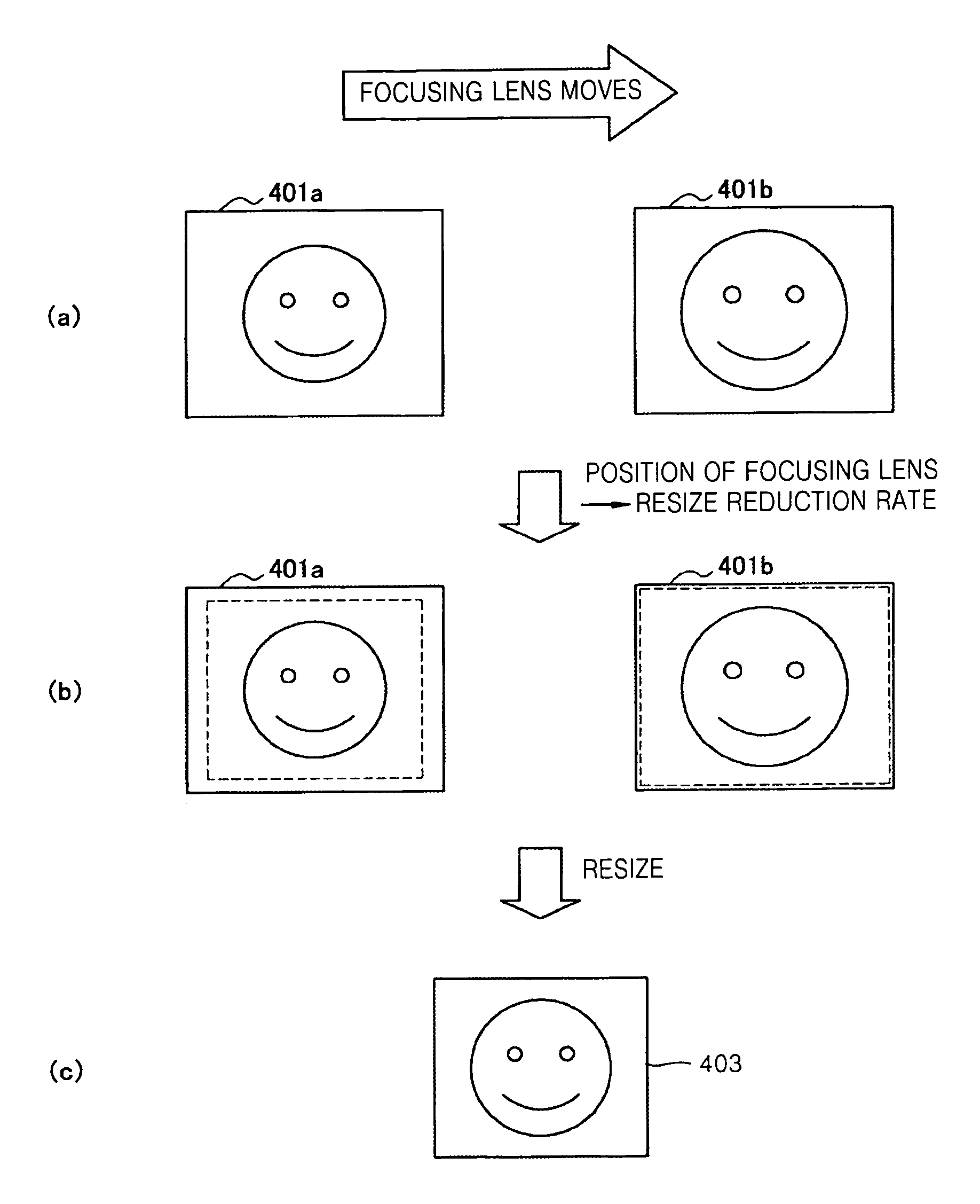
[0033]The present invention will now be described more fully with reference to the accompanying drawings, in which exemplary embodiments of the invention are shown. Like reference numerals in the drawings denote like elements, and thus descriptions of like elements will not be repeated.

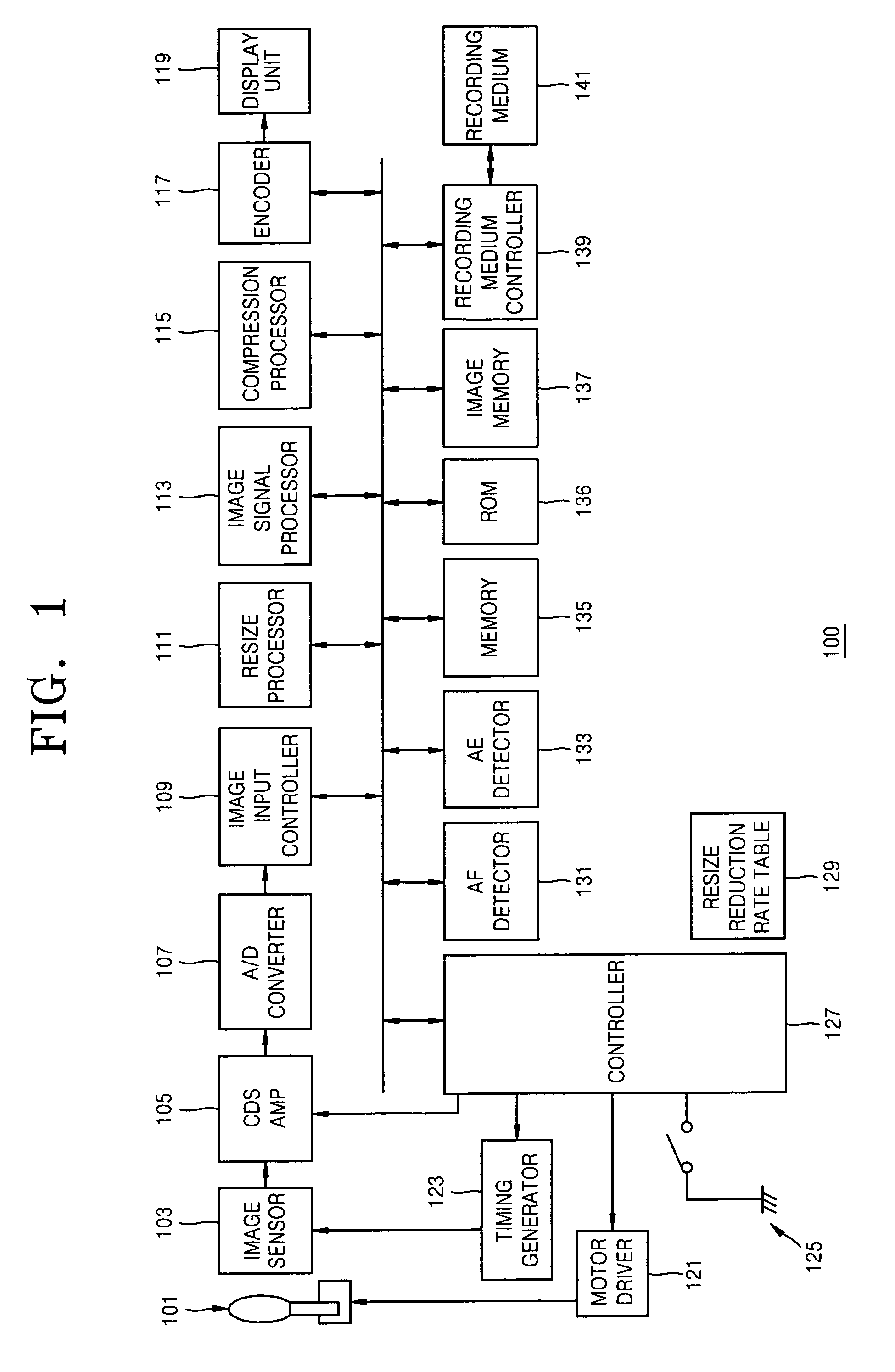
[0034]FIG. 1 is a schematic block diagram of an example imaging device 100 according to an embodiment of the present invention.

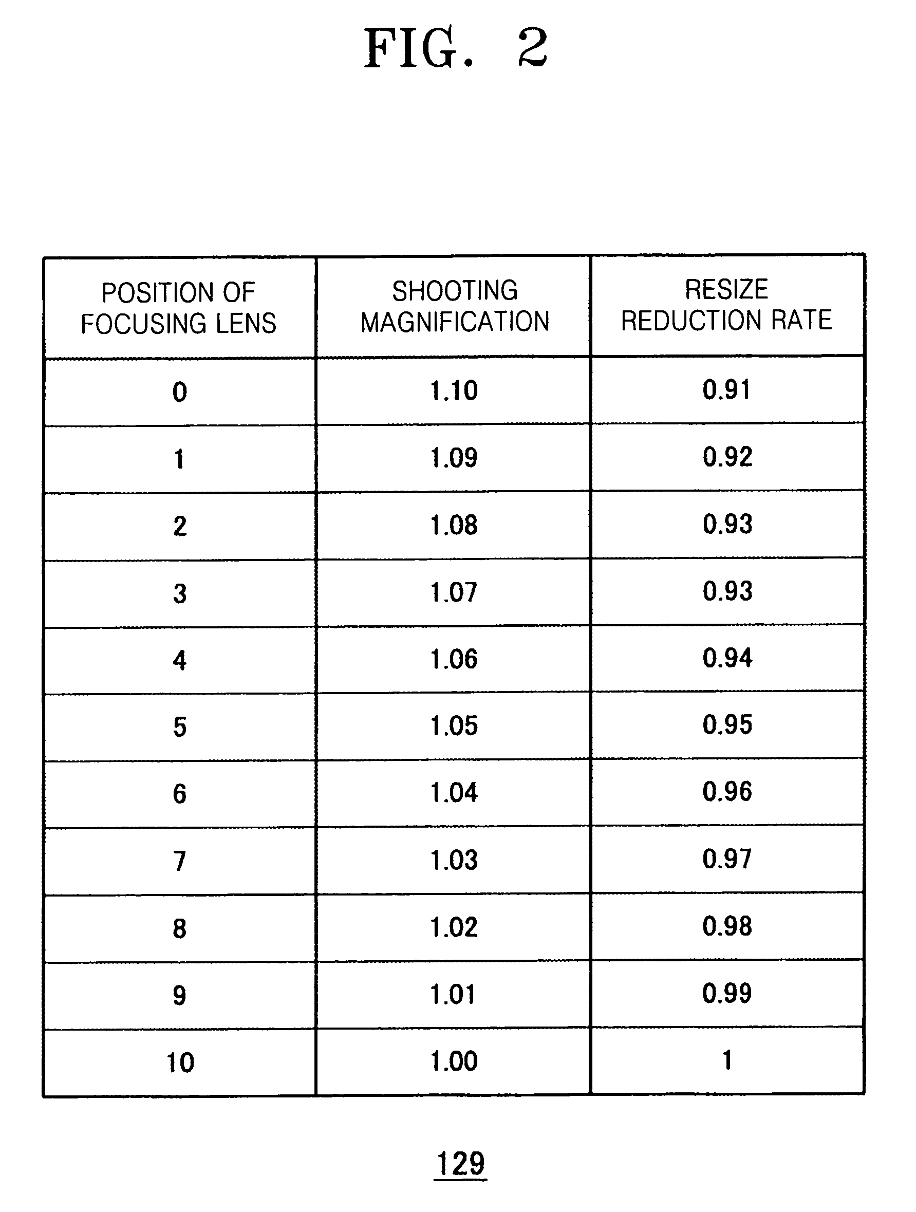
[0035]Referring to FIG. 1, the imaging device 100 includes: a focusing lens 101; an image sensor 103; a correlated double sampling amplifier (CDSAMP) 105; an analog / digital (A / D) converter 107; an image input controller 109; a resize processor 111 or a size changer; an image signal processor 113; a compression processor 115; an encoder 117; a display unit 119; a motor driver 121; a timing generator 123; a switch 125; a controller 127, which may include a magnification changing rate obtaining unit; a resize reduction rate table 129; an automatic focus (AF) detector 131 or an AF...


PUM


Abstract

An imaging device is provided. The imaging device can maintain a constant angle of view even if a focal distance of an entire lens system changes as a focusing lens moves. The imaging device includes an image sensor, a focusing lens, a lens driver, an image generator, a magnification changing rate obtaining unit, and a size changer. The image sensor shoots a snap shot of an object, and the focusing lens performs focusing on the object. The lens driver drives the focusing lens to a plurality of focal points for the object, and the image generator generates an image on the basis of a photograph signal from the image sensor. The magnification changing rate obtaining unit obtains a magnification changing rate for each focal point such that an angle of view for each image photographed at each focal point of the focusing lens is maintained constant. The size changer changes the size of the image on the basis of the magnification changing rate.

Description

CROSS-REFERENCE TO RELATED PATENT APPLICATION[0001]This application claims the benefit of Japanese Patent Application No. 2005-0336082, filed on Nov. 21, 2005, in the Japanese Intellectual Property Office, the disclosure of which is incorporated herein in its entirety by reference.BACKGROUND OF THE INVENTION[0002]1. Field of the Invention[0003]The present invention relates to an imaging device and an image processing method.[0004]2. Description of the Related Art[0005]In imaging devices such as still cameras there has been a problem in that when focusing is performed at a very long or short distance by a focusing lens of a lens optical system, an angle of view changes in order to vary a focal distance of an entire lens system.[0006]One imaging device capable of solving this problem and that is able to maintain a constant angle of view is disclosed in Japanese Patent No. 2503442 and includes a correction apparatus that is additionally added to a lens optical system to maintain a cons...

Claims


Application Information

Patent Timeline
Patent Type & Authority Patents(United States)
IPC IPC(8): H04N5/232G03B13/00H04N5/262
CPCH04N5/232H04N5/23212H04N5/23296H04N5/2351H04N5/2353H04N5/238H04N23/673H04N23/635H04N23/69H04N23/75H04N23/71H04N23/73H04N23/67
Inventor GOTANDA, YOSHIHARU
Owner SAMSUNG ELECTRONICS CO LTD
Why Eureka
Try Eureka