Camera module package

a technology of camera module and camera body, which is applied in the field of camera module package, can solve the problems of unfavorable image sensor module height, increased size of entire module, and need for additional process, so as to prevent tilting or rotating of optical axis, the effect of decreasing the height of the image sensor modul

Active Publication Date: 2010-02-16
SAMSUNG ELECTRO MECHANICS CO LTD
View PDF28 Cites 35 Cited by
  • Summary
  • Abstract
  • Description
  • Claims
  • Application Information

AI Technical Summary

Benefits of technology

[0018]An advantage of the present invention is that it provides a camera module package which can prevent such reliability defects that a chip is damaged by stress applied to an image sensor at reliability evaluation such as a falling test even when the thickness of the image sensor is reduced by decreasing the height of an image sensor module.
[0019]Additional aspect and advantages of the present general inventive concept will be set forth in part in the description which follows and, in part, will be obvious from the description, or may be learned by practice of the general inventive concept.
[0020]According to an aspect of the invention, a camera module package comprises a housing having a lens section mounted therein; a circuit board having a window through which light transmitted through the lens section of the housing passes; an image sensor that is flip-chip bonded to a lower surface of the circuit board; and an impact absorbing member attached to an upper surface of the circuit board, of which the side surface serves as a coupling guide which is coupled to an inner periphery of the housing. Since the side surface of the impact absorbing member is coupled to the inner periphery of the housing such that they form a connecting interface, the impact absorbing member directly absorbs or buffers an external impact occurring at a falling test or the like, thereby protecting the ultra-slim image sensor.
[0021]According to another aspect of the invention, the outer circumference of the impact absorbing member is larger than that of the image sensor. In this case, the image sensor does not come in contact with the housing, when the image sensor is coupled to the housing. Therefore, an external impact is prevented from being transmitted to the image sensor.
[0022]According to a further aspect of the invention, a sealing material is filled between the housing and the image sensor bonded to the circuit board, which makes it possible to protect the light receiving surface of the image sensor from the external environment.
[0023]According to a still further aspect of the invention, the outer circumference of the impact absorbing member has the same size as that of the image sensor. Therefore, an image sensor module can be manufactured to have a size corresponding to the size of the image sensor, which makes it possible to manufacture a chip-scale sized package. Further, the outer periphery of the image sensor serves as a coupling guide so as to prevent tilting or rotating of an optical axis which occurs at the time of packaging.

Problems solved by technology

However, since wire should be used for the connection with a PCB, the size of the entire module increases and an additional process is needed.
Therefore, it is unfavorable in terms of the height of the image sensor module.
However, when the thickness of an image sensor is drastically reduced in order to make an image sensor module ultra-slim, a chip can be damaged by stress which is applied to the image sensor at reliability evaluation such as a falling test.
Therefore, reliability problems such as damage of a chip still remain.
Further, in a conventional COF packing method, such elements as multilayer ceramic capacitors (MLCC) cannot be mounted so as to be positioned inside the housing of the camera module because of the IR filter attached to the FPCB, but are inevitably mounted so as to be positioned on the same surface as the surface, on which the image sensor is attached, or outside the housing.
As a result, the required FPCB increases in size, thereby increasing the size of the entire image sensor module.

Method used


Image

  • Camera module package
  • Camera module package
  • Camera module package

Examples


Embodiment Construction

[0042]Reference will now be made in detail to the embodiments of the present general inventive concept, examples of which are illustrated in the accompanying drawings, wherein like reference numerals refer to like elements throughout. The embodiments are described below in order to explain the present general inventive concept by referring to the figures.

[0043]Hereinafter, a preferred embodiment of the present invention will be described in detail with reference to the accompanying drawings.

[0044]Camera Module Package

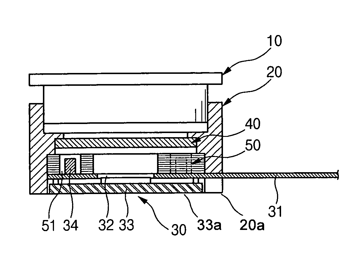
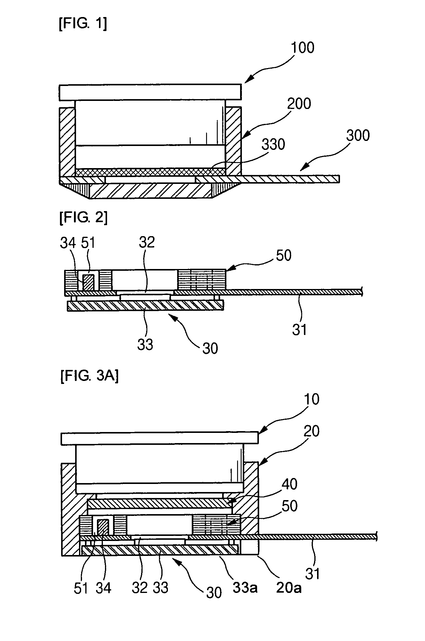
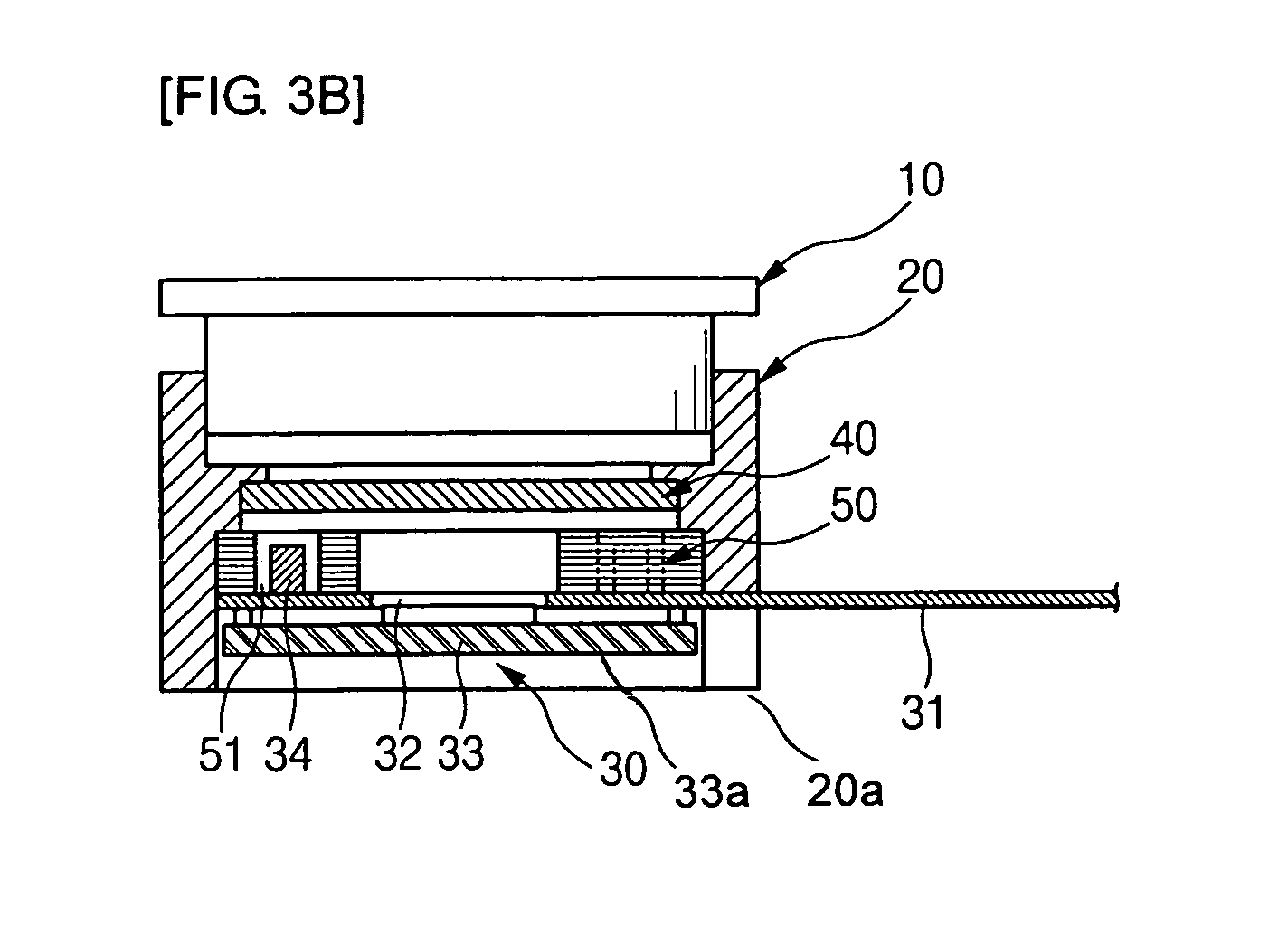
[0045]FIG. 2 is a front view illustrating an image sensor module according to the invention, FIGS. 3A and 3B are front views illustrating a camera module package including the image sensor module, FIG. 4 is an exploded perspective view illustrating the camera module package according to the invention, FIGS. 5A to 5C are diagrams illustrating various examples of an impact absorbing member, and FIGS. 6A and 6B are diagram illustrating various examples depending on a relat...


PUM


Abstract

A camera module package comprises a housing having a lens section mounted therein; a circuit board having a window through which light transmitted through the lens section of the housing passes; an image sensor that is flip-chip bonded to a lower surface of the circuit board; and an impact absorbing member attached to an upper surface of the circuit board, of which the side surface serves as a coupling guide which is coupled to an inner periphery of the housing.

Description

CROSS-REFERENCE TO RELATED APPLICATIONS[0001]This application claims the benefit of Korean Patent Application No. 2006-24116 filed with the Korea Industrial Property Office on Mar. 15, 2006, the disclosure of which is incorporated herein by reference.BACKGROUND OF THE INVENTION[0002]1. Field of the Invention[0003]The present invention relates to a camera module package including an image sensor module which is used in digital cameras, mobile equipments or various monitoring devices, and more specifically, to an ultra-small-sized camera module package which can obtain an excellent result at a falling test even when an ultra-slim image sensor is used.[0004]2. Description of the Related Art[0005]As the information communication technology rapidly develops, data communication speed is improved, and an amount of data communication is expanded. Further, an imaging device such as a CCD image sensor or CMOS image sensor is mounted on mobile electronic equipments such as mobile phones or not...

Claims


Application Information

Patent Timeline
Patent Type & Authority Patents(United States)
IPC IPC(8): G03B17/00H04N5/225
CPCG03B17/00H04N5/2253H04N5/2254H04N5/2257H04N23/54H04N23/57H04N23/55H04N23/00H04N25/00
Inventor CHO, JAE SUBKIM, JUNG JIN
Owner SAMSUNG ELECTRO MECHANICS CO LTD
Why Eureka
Try Eureka