Pixel sensor with reduced image lag

a pixel sensor and image lag technology, applied in the field of semiconductor structure, can solve problems such as signal loss of current image, and achieve the effect of lowering potential barriers

Active Publication Date: 2010-06-08
GLOBALFOUNDRIES U S INC
View PDF5 Cites 4 Cited by
  • Summary
  • Abstract
  • Description
  • Claims
  • Application Information

AI Technical Summary

Benefits of technology

[0008]To address the needs described above, the present invention provides a CMOS image sensor structure having a body with a tensile stress between a charge collection well of a photodiode and a floating drain to lower a potential barrier between the source region and the body, and methods of manufacturing the same.
[0009]In the present invention, a tensile-stress-generating structure is formed above a gate electrode in a CMOS image sensor to apply a normal tensile stress between a charge collection well of a photodiode, which is also a source region of a transfer transistor, and a floating drain in the direction connecting the source region and the floating drain. The tensile stress lowers the potential barrier between the source region and the body of the transfer transistor to effect a faster and more through transfer of the electrical charges in the source region to the floating drain. Image lag is thus reduced in the CMOS image sensor. Further, charge capacity of the source region is also enhanced due to the normal tensile stress applied to the source region.

Problems solved by technology

The image lag causes signal loss for a current image.

Method used


Image

  • Pixel sensor with reduced image lag
  • Pixel sensor with reduced image lag
  • Pixel sensor with reduced image lag

Examples


Embodiment Construction

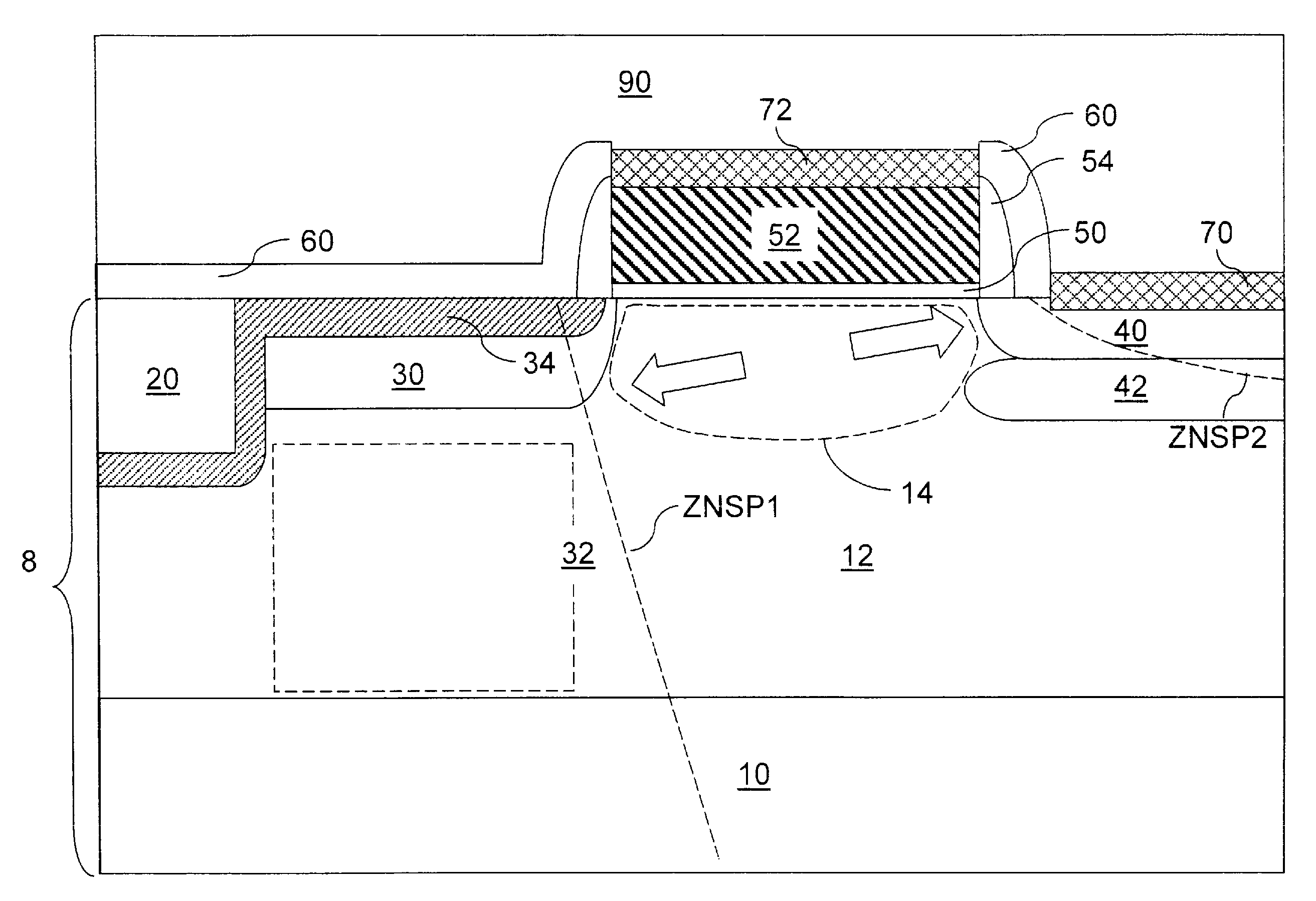
[0051]As stated above, the present invention relates to a complementary metal oxide semiconductor (CMOS) image sensor structure having reduced image lag and enhanced capacitance, and methods of manufacturing the same, which are now described in detail with accompanying figures. It is noted that like and corresponding elements are referred to by like names or reference numerals in the figures.

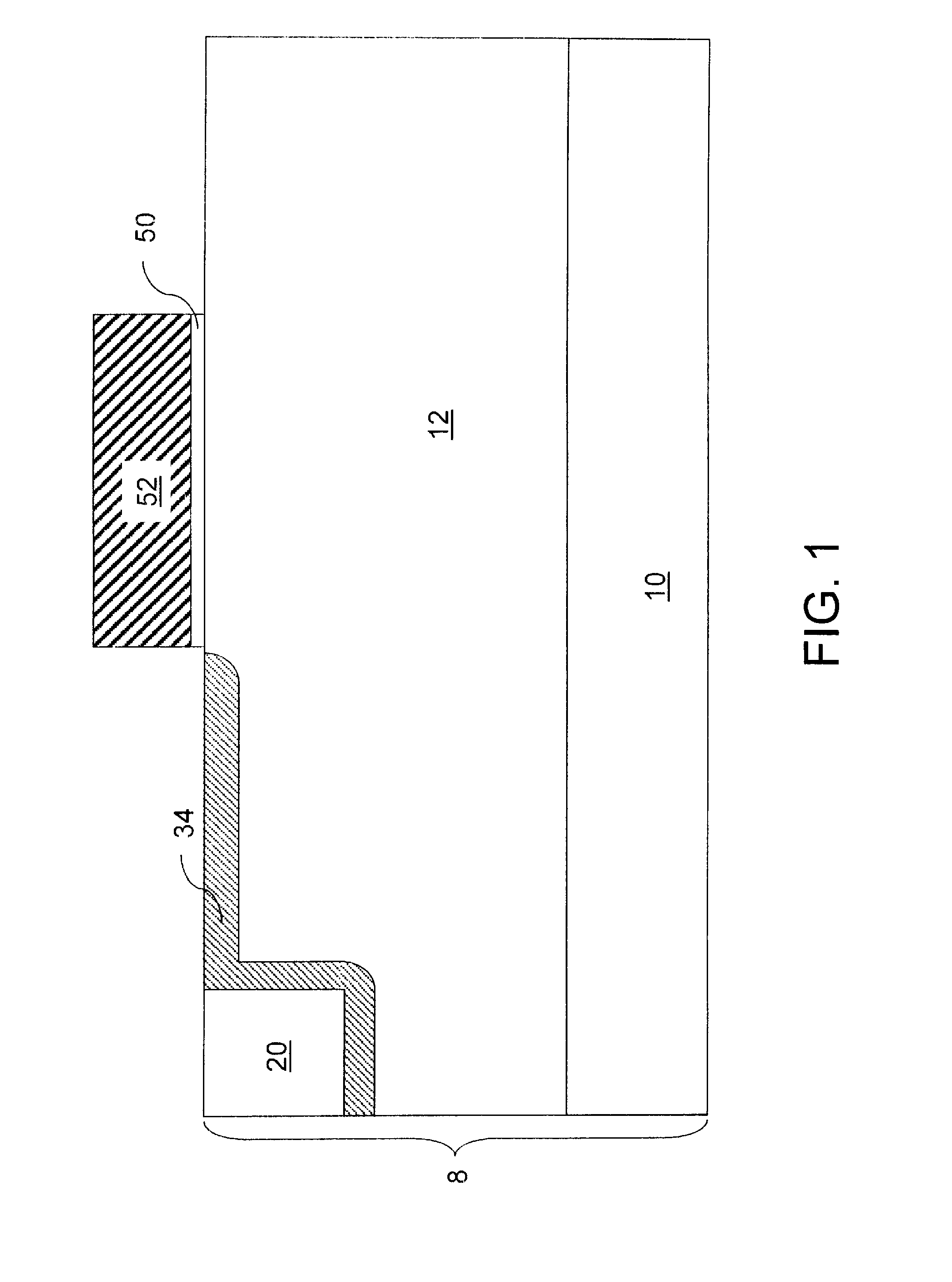
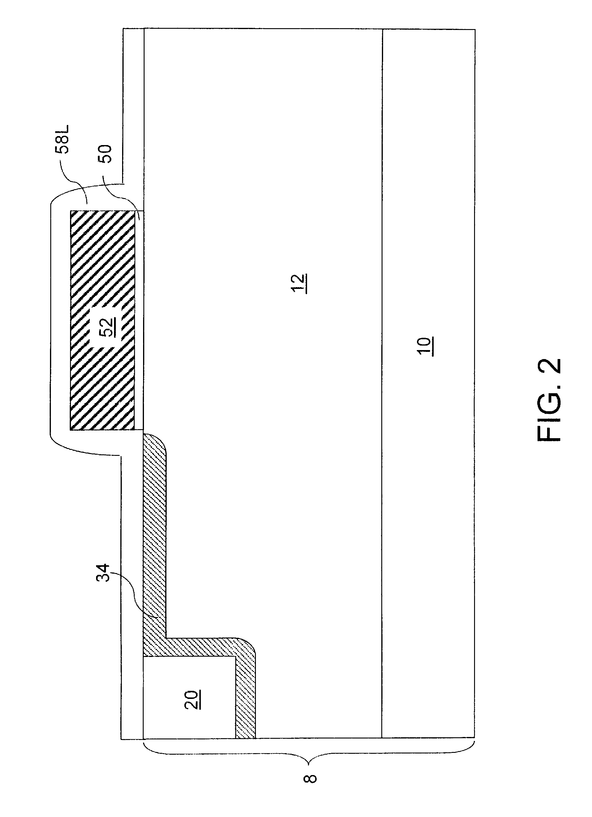
[0052]Referring to FIG. 1, a first exemplary semiconductor structure, which constitutes a portion of a CMOS image sensor pixel, includes a semiconductor substrate 8 and a transfer gate transistor formed thereupon. The semiconductor substrate 8 comprises a heavily-doped first conductivity type semiconductor layer 10, a lightly-doped first conductivity type semiconductor layer 12, and a shallow trench isolation structure 20. The semiconductor substrate 8 further comprises a surface pinning layer 34.

[0053]In the present invention, a lightly-doped semiconductor material denotes a semiconductor mater...


PUM


Abstract

A tensile-stress-generating structure is formed above a gate electrode in a CMOS image sensor to apply a normal tensile stress between a charge collection well of a photodiode, which is also a source region of a transfer transistor, and a floating drain in the direction connecting the source region and the floating drain. The tensile stress lowers the potential barrier between the source region and the body of the transfer transistor to effect a faster and more through transfer of the electrical charges in the source region to the floating drain. Image lag is thus reduced in the CMOS image sensor. Further, charge capacity of the source region is also enhanced due to the normal tensile stress applied to the source region.

Description

FIELD OF THE INVENTION[0001]The present invention relates to a semiconductor structure, and particularly to a pixel sensor cell structure having reduced image lag and enhanced capacitance, and methods of manufacturing the same.BACKGROUND OF THE INVENTION[0002]An image sensor converts a visual image to digital data that may be represented by a picture. The image sensor comprises an array of pixel sensor cells, which are unit devices for the conversion of the visual image into the digital data. Digital cameras and optical imaging devices employ an image sensor. Image sensors include charge-coupled devices (CCDs) or complementary metal oxide semiconductor (CMOS) image sensors.[0003]While CMOS image sensors have been more recently developed compared to the CCDs, CMOS image sensors provide an advantage of lower power consumption, smaller size, and faster data processing than CCDs as well as direct digital output that is not available in CCDs. Also, CMOS image sensors have lower manufactu...

Claims


Application Information

Patent Timeline
Patent Type & Authority Patents(United States)
IPC IPC(8): H01L31/062
CPCH01L27/14603
Inventor ADKISSON, JAMES WGAMBINO, JEFFREY P.KRISHNASAMY, RAJENDRANMULUGETA, SOLOMON
Owner GLOBALFOUNDRIES U S INC
Why Eureka
Try Eureka