Semiconductor device manufacturing method

A semiconductor and substrate technology, applied in the field of manufacturing semiconductor devices, can solve problems such as affecting transistor performance, and achieve the effects of improving device performance and alleviating short channel effects

Active Publication Date: 2019-01-15
TAIWAN SEMICON MFG CO LTD
View PDF6 Cites 1 Cited by
  • Summary
  • Abstract
  • Description
  • Claims
  • Application Information

AI Technical Summary

Problems solved by technology

In advanced process technology, when the channel length of the transistor reaches the same level as the width of the depletion layer, the short channel effect will occur and adversely affect the transistor performance

Method used


Image

  • Semiconductor device manufacturing method
  • Semiconductor device manufacturing method
  • Semiconductor device manufacturing method

Examples


Embodiment Construction

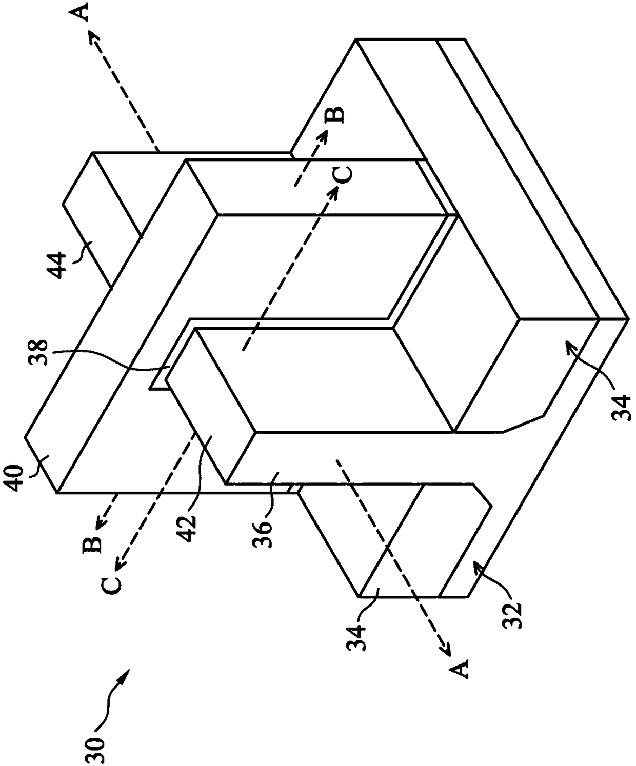
[0065] Different embodiments or examples provided below may implement different configurations of the present invention. The examples of specific components and arrangements are used to simplify the invention and not to limit the invention. For example, the statement that the first component is formed on the second component includes that the two are in direct contact, or there are other additional components interposed between the two instead of direct contact. In addition, the numbers and / or symbols may be repeated in various examples of the present invention, but these repetitions are only for simplification and clarity of description, and do not mean that units with the same number and / or symbols between different embodiments and / or configurations have the same correspondence.

[0066] In addition, spatial relative terms such as "below", "below", "lower side", "above", "upper side" or similar terms may be used to simplify describing the relative relationship of one elemen...


PUM


Abstract

A method includes providing a substrate having a gate structure over a first side of the substrate, forming a recess adjacent to the gate structure, and forming in the recess a first semiconductor layer having a dopant, the first semiconductor layer being non-conformal, the first semiconductor layer lining the recess and extending from a bottom of the recess to a top of the recess. The method further includes forming a second semiconductor layer having the dopant in the recess and over the first semiconductor layer, a second concentration of the dopant in the second semiconductor layer being higher than a first concentration of the dopant in the first semiconductor layer.

Description

technical field [0001] Embodiments of the present invention relate to fabricating semiconductor devices, and more particularly to forming contacts (also called contact plugs) in semiconductor devices. Background technique [0002] The semiconductor integrated circuit industry has experienced rapid growth due to continuous improvements in the integration density of various electronic components such as transistors, diodes, resistors, capacitors, or the like. The main improvement of the above-mentioned integration density is to continuously reduce the size of the smallest structure, so that more components can be integrated into a limited area. [0003] Transistor size shrinks, shrinking the size of each structure. In advanced process technology, when the channel length of the transistor reaches the same level as the width of the depletion layer, the short channel effect will occur and adversely affect the performance of the transistor. This technical field requires structur...

Claims


Application Information

Patent Timeline
Patent Type & Authority Applications(China)
IPC IPC(8): H01L21/336H01L29/06
CPCH01L29/0684H01L29/66795H01L23/485H01L21/02381H01L21/0245H01L21/02576H01L21/02579H01L21/0262H01L21/02639H01L29/6653H01L29/7848H01L29/0847H01L29/165H01L21/02532H01L29/66545H01L29/785H01L29/66348H01L29/6656H01L23/53257H01L21/76843H01L21/76871H01L23/5226H01L21/823418H01L21/823431
Inventor 马志宇沙哈吉·B·摩尔李承翰潘正扬张世杰
Owner TAIWAN SEMICON MFG CO LTD
Why Eureka
Try Eureka