Method of making a depleted poly-silicon edged MOSFET structure

a poly-silicon edged mosfet and poly-silicon technology, applied in the field of semiconductor structures, can solve the problems of increasing the complexity of manufacturing requirements, affecting the performance of devices, and affecting the corner device i.e., the channel region under the gate conductor at the corners of the trenches

Inactive Publication Date: 2000-08-08
IBM CORP
View PDF30 Cites 38 Cited by
  • Summary
  • Abstract
  • Description
  • Claims
  • Application Information

AI Technical Summary

Problems solved by technology

As the widths of these devices are made smaller, unwanted effects originating at the corner device i.e., the channel region under gate conductor at the corners of the trenches, become more significant.
This lower threshold voltage provides a parallel path for current conduction which has different turn-on characteristics and adversely affects the performance of the device.
While such techniques have been found to reduce the threshold voltage of the corner device, they provide other problems such as increasing the complexity of manufacturing requirements or requiring an undesirable increase in the thickness of layers.
Some of the prior art techniques have caused an increase in voltage threshold away from the corners as well.

Method used


Image

  • Method of making a depleted poly-silicon edged MOSFET structure
  • Method of making a depleted poly-silicon edged MOSFET structure
  • Method of making a depleted poly-silicon edged MOSFET structure

Examples


first embodiment

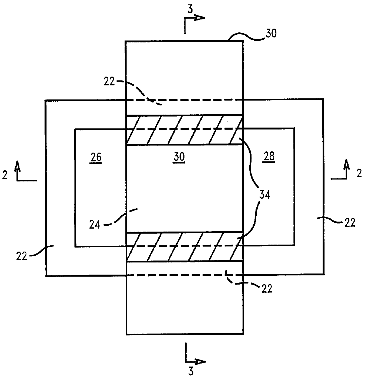
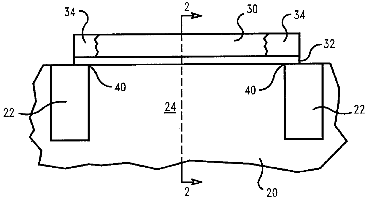
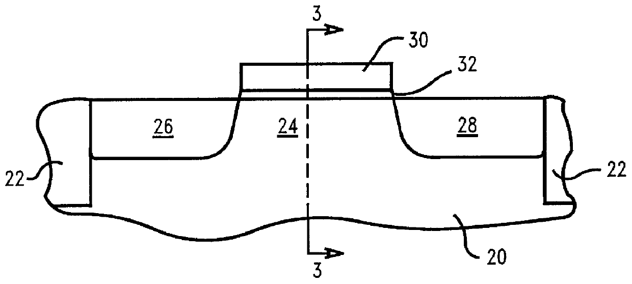
In the method of the present invention, FIGS. 9, 10 and 11 show a method of polysilicon edge depletion using blocked source / drain implants. In FIG. 9, extension implants 27, 29 comprise low doped transistor implants for the source and drain, respectively. These extension implants are closer to the gate 30 and dielectric 32 than the subsequent source 26 and drain 28 implant regions formed in FIGS. 10 and 11. The source / drain extension implants are formed at lower energy and dose levels than the source / drain implants, which extend deeper into the substrate. Extension implants 27, 29 overlap with the subsequent source and drain implants 26, 28 and may extend under the gate and dielectric layers somewhat. As shown in FIG. 11, the formation of the source and drain implants 26, 28 is made after forming a mask layer 38 which exposes the central portion of the surface of gate layer 30, but shields the edge regions. Mask 38 blocks the implant of n- or p-type dopants 50 from the corner region...

second embodiment

In the method shown in FIGS. 12 and 13, the method uses complimentary source / drain implants to counterdope the corner regions of the gate. Extension regions 27 and 29 are otherwise conventionally formed (FIG. 12) using low energy and dose n- or p- type implants. In an NFET device, hereafter the deeper source and drain regions and gate 30 are simultaneously doped throughout with an n-type dopant. A p-type source drain mask 38' is then applied over the source and drain regions and the entire upper surface of the gate and isolation structures, except for the opposite gate 30 edges and portions of the spacers 34, which remain unmasked (FIG. 13). A p-type dopant 51 is then implanted into the gate corner region to produce regions 34 which are counterdoped to the n-type dopant in the remainder of the gate layer 30. Processing then may continue as described previously. In a PFET device, the dopants described previously are reversed.

third embodiment

the method of the present invention is shown in FIGS. 14 and 15, in which the method uses complimentary extension implants to counterdope the corner regions near the gate edges. In an NFET device, an n-type dopant 52 is implanted at low energy and dose levels in the source and drain extension regions and also throughout the gate layer 30, as shown in FIG. 14. Thereafter, a p-type source drain mask 38" is then applied over the source and drain extension regions and also over the entire upper surface of the gate and isolation structures, except for the drain extension region and the opposite gate 30 edges and portions of the spacers 34, which remain unmasked (FIG. 15). A p-type dopant 51 is then implanted into the gate edges to produce gate regions 34 which are counterdoped to the n-type dopant in the remainder of the gate layer 30. The n-type dopant is applied to form the source and drain regions 26, 28, without further affecting the gate 30 and counterdoped corner regions 34. Proces...


PUM


Abstract

A field effect transistor with reduced corner device problems comprises source and drain regions formed in a substrate, a channel region between the source and drain regions, isolation regions in the substrate adjacent the source, channel and drain regions; and a gate having a gate dopant over the channel region and separated therefrom by a gate dielectric. The isolation regions define corner regions of the channel along interfaces between the channel and isolation regions. The gate includes regions depleted of the gate dopant and overlapping at least the channel region and the isolation regions, such that voltage thresholds of the channel corner regions beneath depleted portions of the gate conductor layer are increased compared to regions of the channel between the corner regions. The field effect transistor with reduced dopant concentration on the MOSFET gate "corner" has an improved edge voltage tolerance. The structure has improved edge dielectric breakdown and lower MOSFET gate-induced drain leakage (GIDL). This structure is intended for analog applications, mixed voltage tolerant circuits and electrostatic (ESD) networks.

Description

1. Field of the InventionThis invention relates to semiconductor structures, and in particular to field effect transistor (FET) devices incorporating depleted zones in the gate conductor along the corner region of the FET to increase the threshold voltage of the corner device.2. Description of Related ArtContemporary CMOS devices employ field effect transistors (FET) which are adjacent to or bounded by trenches such as shallow trench isolation (STI). As the widths of these devices are made smaller, unwanted effects originating at the corner device i.e., the channel region under gate conductor at the corners of the trenches, become more significant. It has been found that the electric field in the gate conductor near the trench corner may become enhanced, which leads to a reduction of the threshold voltage of the channel in that region, compared to the threshold voltage of the channel under the planar portion of the gate away from the corner. This lower threshold voltage provides a p...

Claims


Application Information

Patent Timeline
Patent Type & Authority Patents(United States)
IPC IPC(8): H01L21/28H01L21/70H01L29/49H01L21/762H01L29/423H01L21/336H01L21/02H01L29/40H01L29/78H01L29/786
CPCH01L29/6659H01L21/28105H01L21/28123H01L21/76224H01L29/4238H01L29/4983Y10S438/919H01L29/78
Inventor BROWN, JEFFREY S.GAUTHIER, JR., ROBERT J.VOLDMAN, STEVEN H.
Owner IBM CORP
Why Eureka
Try Eureka