Method of manufacturing semiconductor device

a manufacturing method and semiconductor technology, applied in the direction of semiconductor devices, electrical appliances, transistors, etc., to achieve the effect of increased thickness of oxide semiconductor films, and less fluctuation in threshold voltag

Active Publication Date: 2014-09-09
SEMICON ENERGY LAB CO LTD
View PDF186 Cites 38 Cited by
  • Summary
  • Abstract
  • Description
  • Claims
  • Application Information

AI Technical Summary

Benefits of technology

[0009]In view of the above problem, an object is to provide a semiconductor device formed using an oxide semiconductor, which has stable electric characteristics and high reliability.
[0016]In a manufacturing process of a transistor including an oxide semiconductor film, oxygen doping treatment is performed, and then heat treatment is performed in a state where an aluminum oxide film which has a function of preventing entry of water (including hydrogen) into the oxide semiconductor film and a function of preventing release of oxygen from the oxide semiconductor film is provided. Consequently, at least one region where oxygen exists at an amount exceeding that in the stoichiometric composition of the oxide semiconductor film (such a region is also referred to as oxygen-excess region) can be provided in the inside (bulk) of the oxide semiconductor film or an interface between an insulating film and the oxide semiconductor film. Note that oxygen which is added by the oxygen doping treatment may exist between lattices of the oxide semiconductor.
[0022]In addition, it has been confirmed that as the thickness of the oxide semiconductor film is increased, fluctuation in the threshold voltage of a transistor tends to increase. It can be guessed that this is because an oxygen defect in the oxide semiconductor film is one cause of the change of the threshold voltage and increases in number as the thickness of the oxide semiconductor film is increased. As described above, in the transistor according to one embodiment of the invention disclosed herein, since the amount of oxygen contained in the oxide semiconductor film is increased by the oxygen doping treatment, an oxygen defect in the film which is caused by the dynamic reaction according to the above formula (I) can be immediately compensated. Accordingly, the transistor according to one embodiment of the invention disclosed herein can have less fluctuation in threshold voltage, because time for formation of a donor level due to an oxygen defect can be shortened and the donor levels can be substantially removed.
[0023]Excess oxygen is contained in an oxide semiconductor film and an aluminum oxide film is provided over the oxide semiconductor film so as to prevent oxygen from being released, whereby it is possible to prevent generation and increase of a defect in the inside of the oxide semiconductor and interfaces between the oxide semiconductor and layers which are over / under and in contact with the oxide semiconductor. In other words, the excess oxygen contained in the oxide semiconductor film functions to fill an oxygen vacancy defect. Accordingly, a semiconductor device having stable electric characteristics and high reliability can be provided.

Problems solved by technology

However, in a semiconductor device including an oxide semiconductor, an oxygen vacancy in the oxide semiconductor might change the electric conductivity thereof.

Method used


Image

  • Method of manufacturing semiconductor device
  • Method of manufacturing semiconductor device
  • Method of manufacturing semiconductor device

Examples


embodiment 1

[0044]In this embodiment, one embodiment of a semiconductor device and a method of manufacturing the semiconductor device will be described with reference to FIGS. 1A to 1C, FIGS. 2A to 2D, and FIGS. 3A to 3C. In this embodiment, a transistor including an oxide semiconductor film will be described as an example of the semiconductor device.

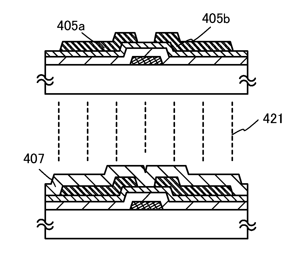
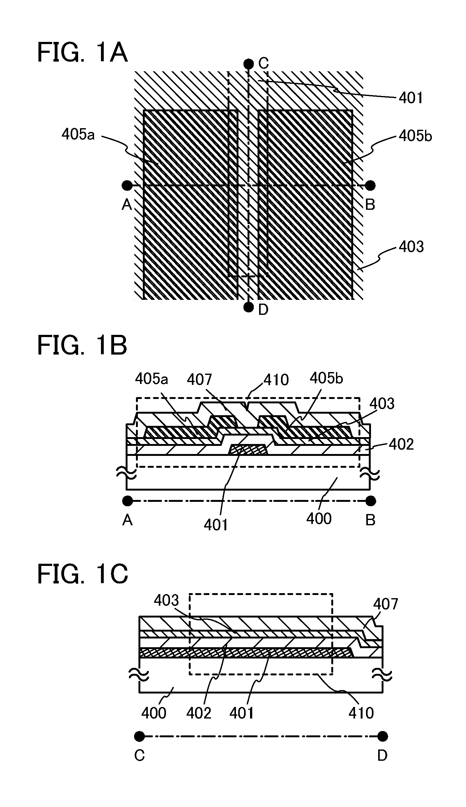
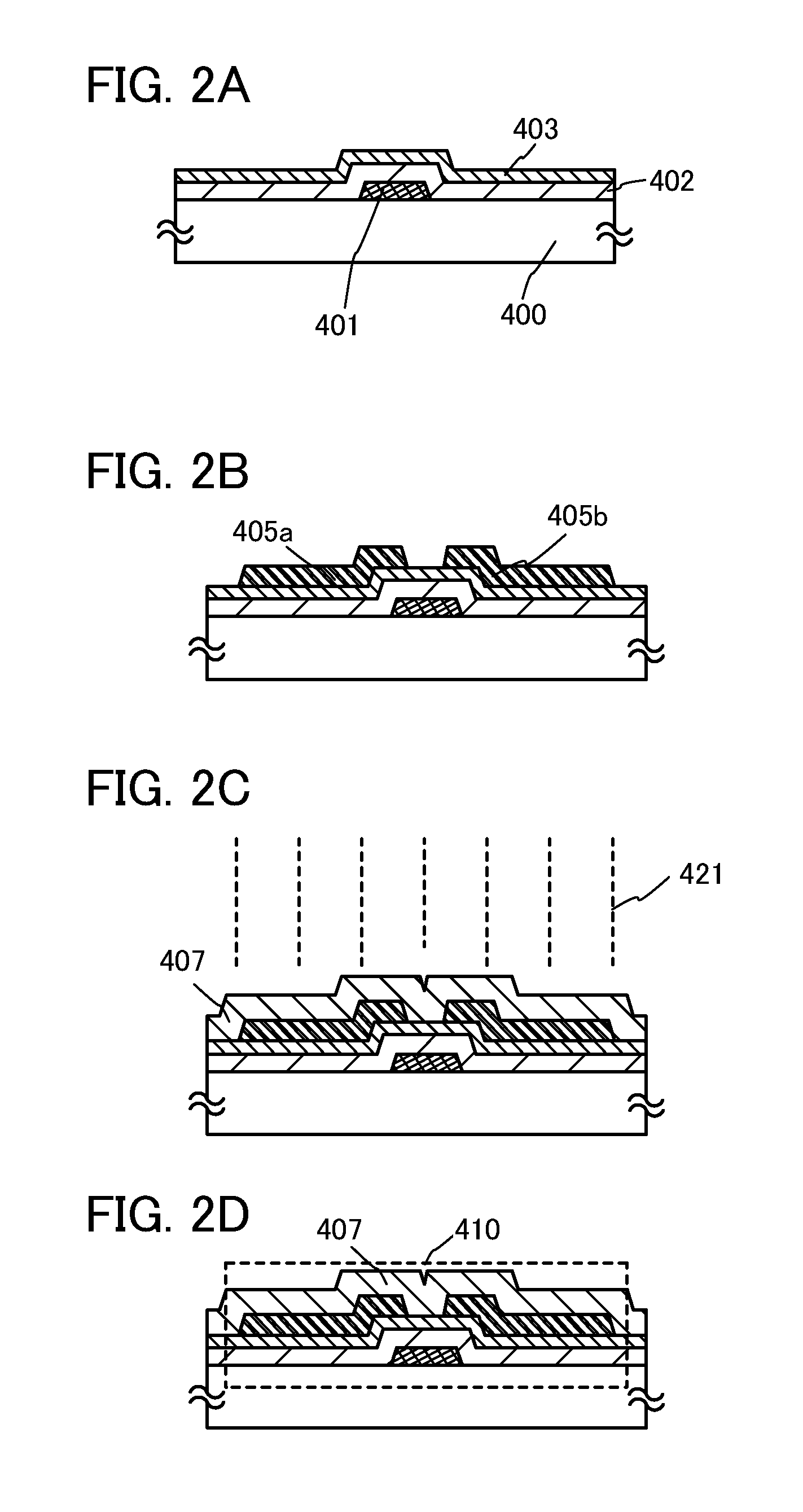
[0045]FIGS. 1A to 1C are a plan view and cross-sectional views which illustrate a bottom-gate transistor 410 as an example of a semiconductor device. FIG. 1A is a plan view, and FIGS. 1B and 1C are cross-sectional views along line A-B and line C-D in FIG. 1A, respectively. Note that in FIG. 1A, some components of the transistor 410 (e.g., an insulating film 407) are omitted for brevity.

[0046]The transistor 410 illustrated in FIGS. 1A to 1C includes, over a substrate 400 having an insulating surface, a gate electrode layer 401, a gate insulating film 402, an oxide semiconductor film 403, a source electrode layer 405a, a drain electrode layer 405b, a...

embodiment 2

[0112]In this embodiment, another embodiment of a semiconductor device and a method of manufacturing the semiconductor device will be described with reference to FIGS. 4A to 4C, FIGS. 5A to 5D, and FIGS. 6A to 6C. Note that the same portions as Embodiment 1 or portions having functions similar to those of Embodiment 1 can be formed as in Embodiment 1, and also the same steps as Embodiment 1 or steps similar to those of Embodiment 1 can be performed as in Embodiment 1; therefore, repetitive description thereof is omitted. In addition, detailed description of the same portions is not repeated.

[0113]FIGS. 4A to 4C are a plan view and cross-sectional views which illustrate a top-gate transistor 510 as an example of a semiconductor device. FIG. 4A is a plan view, and FIGS. 4B and 4C are cross-sectional views along line I-J and line K-L in FIG. 4A, respectively. Note that in FIG. 4A, some components of the transistor 510 (e.g., the insulating film 407) are omitted for brevity.

[0114]The tr...

embodiment 3

[0139]A semiconductor device having a display function (also referred to as display device) can be manufactured using the transistor described in Embodiment 1 or 2. Moreover, some or all of driver circuits which include transistors can be formed over a substrate where a pixel portion is formed, whereby a system-on-panel can be obtained.

[0140]In FIG. 8A, a pixel portion 4002 provided over a first substrate 4001 is sealed by a second substrate 4006 and a sealant 4005 provided so as to surround the pixel portion 4002. In FIG. 8A, a signal line driver circuit 4003 and a scan line driver circuit 4004 which are each formed using a single crystal semiconductor film or a polycrystalline semiconductor film over a substrate prepared separately are mounted in regions that are different from the region surrounded by the sealant 4005 over the first substrate 4001. Various signals and potentials are supplied to the signal line driver circuit 4003, the scan line driver circuit 4004, and the pixel ...


PUM


Abstract

In a manufacturing process of a transistor including an oxide semiconductor film, oxygen doping treatment is performed on the oxide semiconductor film, and then heat treatment is performed on the oxide semiconductor film and an aluminum oxide film provided over the oxide semiconductor film. Consequently, an oxide semiconductor film which includes a region containing more oxygen than a stoichiometric composition is formed. The transistor formed using the oxide semiconductor film can have high reliability because the amount of change in the threshold voltage of the transistor by a bias-temperature stress test (BT test) is reduced.

Description

BACKGROUND OF THE INVENTION[0001]1. Field of the Invention[0002]The present invention relates to a semiconductor device and a method of manufacturing the semiconductor device.[0003]In this specification, a semiconductor device generally means a device which can function by utilizing semiconductor characteristics, and an electrooptic device, a semiconductor circuit, and an electronic appliance are all semiconductor devices.[0004]2. Description of the Related Art[0005]A technique by which transistors are formed using semiconductor thin films over a substrate having an insulating surface has been attracting attention. Such transistors are applied to a wide range of electronic devices such as an integrated circuit (IC) and an image display device (display device). A silicon-based semiconductor material is widely known as a material for a semiconductor thin film applicable to a transistor. As another material, an oxide semiconductor has been attracting attention.[0006]For example, a tran...

Claims


Application Information

Patent Timeline
Patent Type & Authority Patents(United States)
IPC IPC(8): H01L21/42H01L21/84H01L21/336H01L27/12H01L29/786
CPCH01L27/1225H01L29/7869H01L21/02664H01L21/02636H01L21/324H01L29/66742H01L21/02565H01L21/02554H01L21/02175H01L21/02252H01L21/383H01L21/40H01L21/477H01L29/66969
Inventor YAMAZAKI, SHUNPEISATO, YUHEISATO, KEIJIMARUYAMA, TETSUNORIKOEZUKA, JUNICHI
Owner SEMICON ENERGY LAB CO LTD
Why Eureka
Try Eureka