Semiconductor Light Emitting Device and Manufacturing Method Thereof

a technology of semiconductors and light emitting devices, which is applied in the direction of semiconductor lasers, solid-state devices, lasers, etc., can solve the problems of accelerating degradation, reducing the performance of devices, and device modules, and not describing in detail how to incline the end face of resist masks, etc., to achieve stable electric characteristics and high intensity

Inactive Publication Date: 2008-06-19
STANLEY ELECTRIC CO LTD
View PDF17 Cites 43 Cited by
  • Summary
  • Abstract
  • Description
  • Claims
  • Application Information

AI Technical Summary

Benefits of technology

[0015]In accordance with one aspect of the disclosed subject matter, a semiconductor light emitting device can have stable electric characteristics, and can emit light with high intensity from the surface of a substrate.
[0016]The semiconductor light emitting device can have at least a first conductive type semiconductor layer, a luminescent layer, and a second conductive type semiconductor layer which are laminated in this order from the side of a substrate. An end face of the first conductive type semiconductor layer can include a first terrace approximately in parallel with the surface of the substrate, and an inclined end face region disposed nearer to the substrate than the first terrace. A reflective first electrode can be disposed in the inclined end face region. Since the first terrace is provided, it is possible to maintain a relatively large distance between the first electrode and the luminescent layer in a direction approximately in parallel with the surface of the substrate, and to bring the first electrode near to the luminescent layer in the direction of thickness. Thus, it is possible to reflect most of the light propagating towards the end face through a semiconductor layer to the substrate. Therefore, it is possible to increase the intensity of light taken out of the substrate.

Problems solved by technology

Accordingly, there is a problem that when a large current is applied for high power output, heat generation causes reduction in the performance of the device (and device module), causes acceleration of degradation thereof, causes breakage thereof, and the like.
The publication, however, does not describe in detail how to incline the end face of the resist mask to the desired angle.
It is difficult, however, to make the distance between the n-type electrode and the end face of the luminescent layer 5 μm or less by a photolithographic technology using a mask aligner, which is generally used in the manufacture of the light emitting device.
Using a stepper makes it possible to make the distance 1 μm or less, but manufacturing costs increase.
When the distance is 1 μm or less, there is a possibility that dust and a burr occurring in a process after that cause the short circuiting.
When difference in a lattice constant between the substrate and the semiconductor layer is large (for example, a combination of a sapphire C-plane substrate and a gallium nitride semiconductor layer), or difference in a thermal expansion coefficient is large, warpage occurs in the substrate.
Thus, it is difficult to transfer a mask pattern with high precision of 1 μm or less even if a stepper is used.
Furthermore, depending on a material of the electrode, electromigration during use or electrochemical migration may cause the short circuiting, when the end portion of the n-type electrode is brought near to the end face of the luminescent layer to a distance of 1 μm or less.
As described above, it is difficult to efficiently reflect light emitted towards the direction of the end face by the n-type electrode on the inclined surface, and maintain electric characteristics.
If the offset position (distance that is to be floated from the resist layer) of the photomask is misaligned, a blurry region of light largely varies, and hence there is a problem that an inclination width and the inclination angle largely vary.
Therefore, it was difficult to form the inclined surface which can precisely reflect light to a desired direction.
This is because the intensity of propagation light traveling in this range is weak.
Thus, if the size of the partition is reduced, the size (die size) of the whole light emitting device contrarily becomes large.

Method used


Image

  • Semiconductor Light Emitting Device and Manufacturing Method Thereof
  • Semiconductor Light Emitting Device and Manufacturing Method Thereof
  • Semiconductor Light Emitting Device and Manufacturing Method Thereof

Examples


Embodiment Construction

[0052]Some exemplary embodiments of the disclosed subject matter will be hereinafter described.

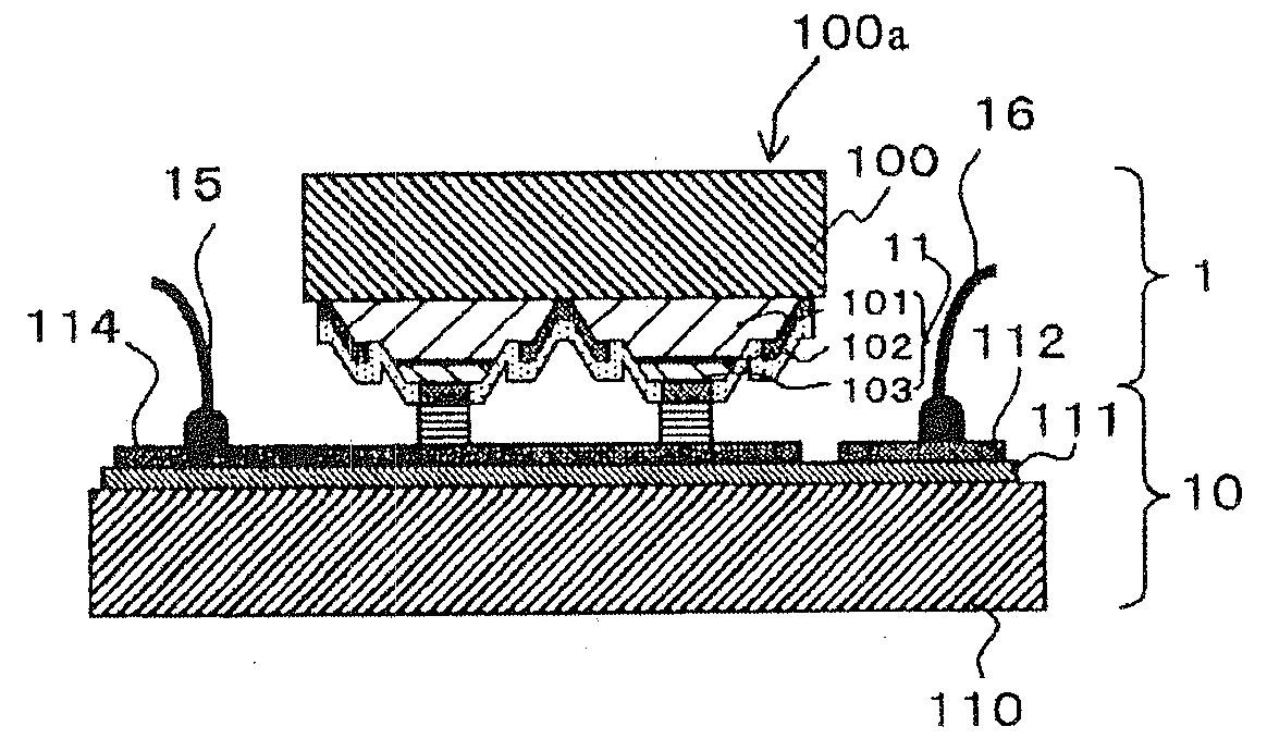
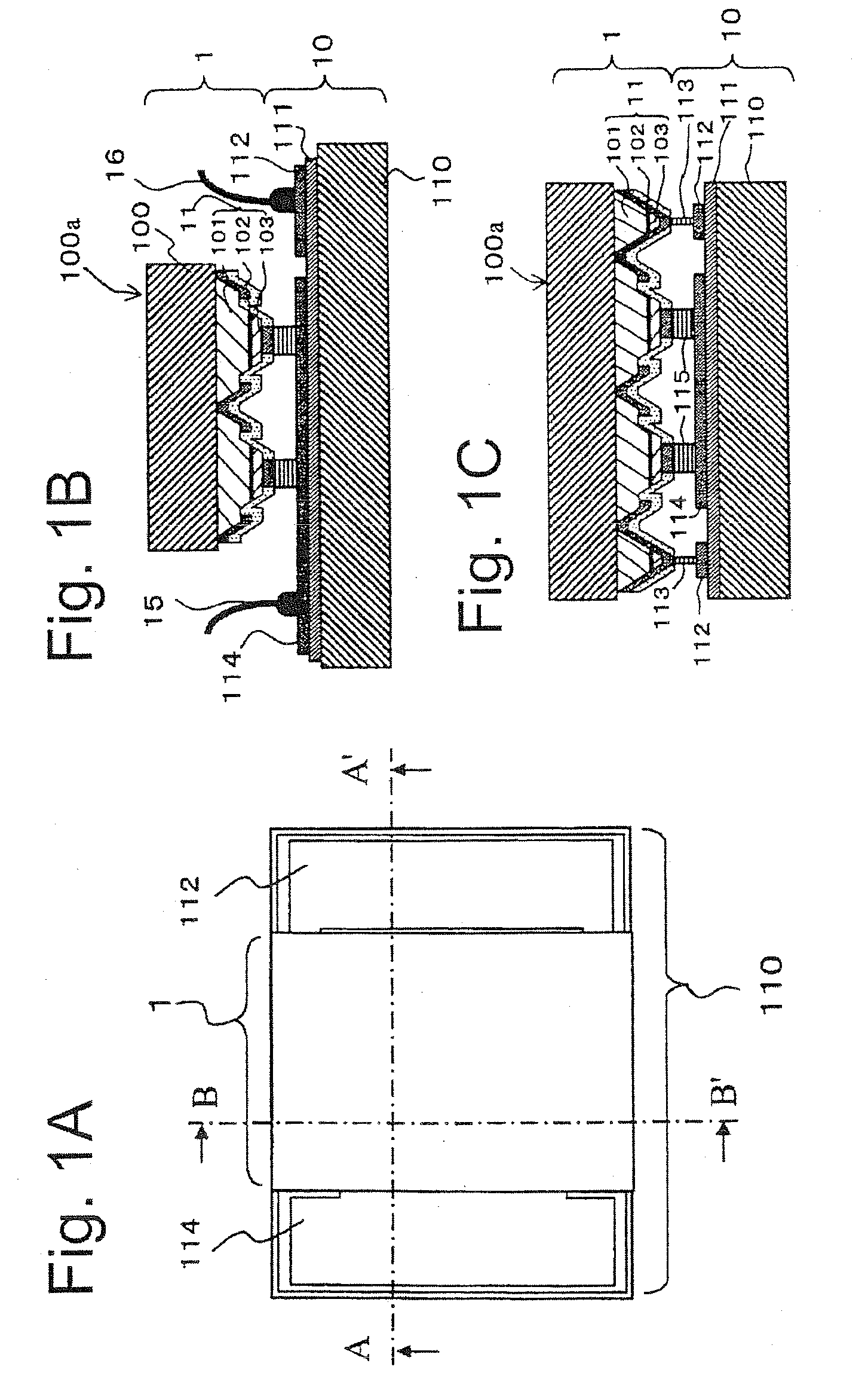
[0053]An embodiment of a semiconductor light emitting device made in accordance with the principles of the disclosed subject matter, as shown in FIGS. 1A to 1C, is a flip chip in which a light emitting device section 1 can be mounted on a support substrate section 10.

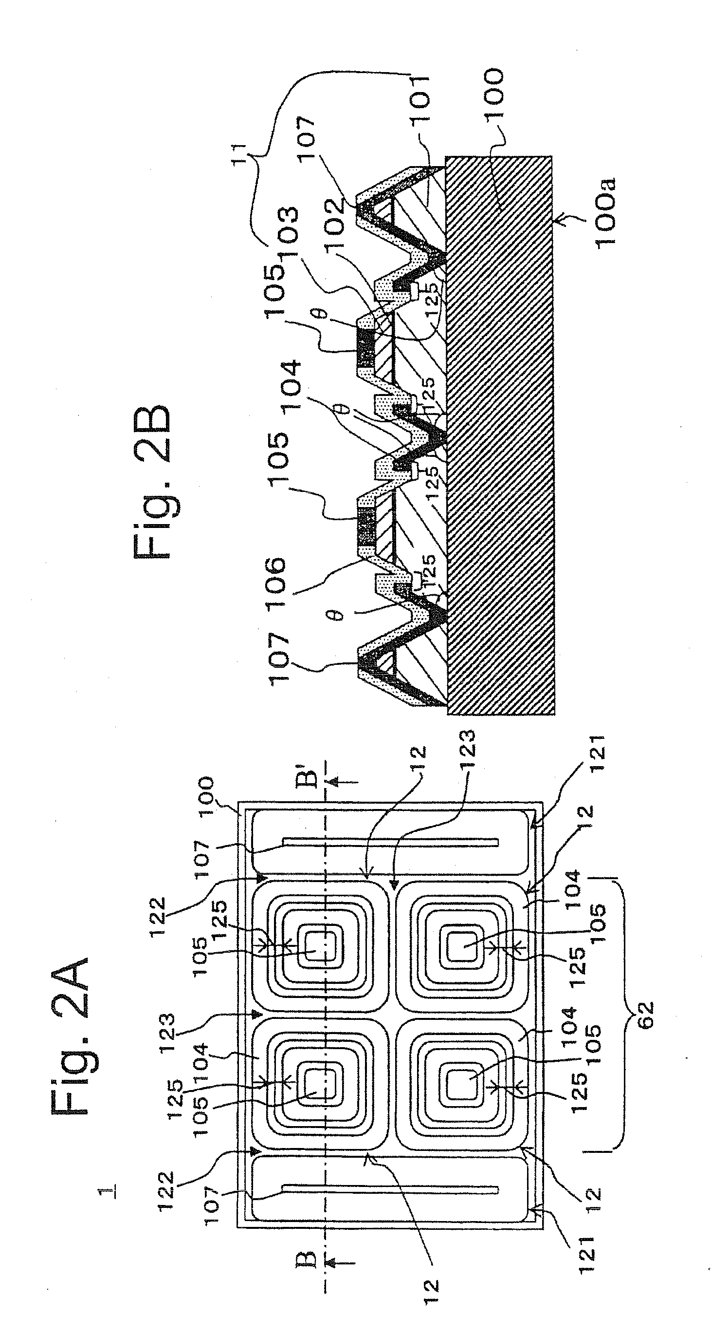
[0054]The structure of the light emitting device section 1 will be described. FIGS. 2A and 2B show the detailed structure of the light emitting device section 1. The light emitting device section 1 can include a sapphire substrate 100, a nitride semiconductor layer 11, electrodes 104 and 105, and a protective film 106. The nitride semiconductor layer 11 includes at least an n-type nitride semiconductor layer 101, a luminescent layer 102, and a p-type nitride semiconductor layer 103 which can be laminated in this order on the sapphire substrate 100. In this example, the nitride semiconductor layer 11 is designed so as to have a...


PUM

PropertyMeasurementUnit
transmittanceaaaaaaaaaa
thermal conductivityaaaaaaaaaa
distanceaaaaaaaaaa

Abstract

A semiconductor light emitting device can have stable electric characteristics and can emit light with high intensity from a substrate surface. The device can include a transparent substrate and a semiconductor layer on the substrate. The semiconductor layer can include a first conductive type semiconductor layer, a luminescent layer, a second conductive type semiconductor layer, and first and second electrodes disposed to make contact with the first and second conductive type semiconductor layers, respectively. The first conductive type semiconductor layer, the luminescent layer, and the second conductive type semiconductor layer can be laminated in order from the side adjacent the substrate. An end face of the semiconductor layer can include a first terrace provided in an end face of the first conductive type semiconductor layer in parallel with the substrate surface, and an inclined end face region provided nearer to the substrate than the first terrace. The first electrode disposed in the inclined end face region can reflect light emitted from the luminescent layer to the substrate.

Description

[0001]This is a divisional application under 35 U.S.C. §120 of U.S. patent application Ser. No. 11 / 154,814, filed Jun. 17, 2005, which in turn claims the priorities benefit under 35 U.S.C. §119 of Japanese Patent Application No. 2004-180915, filed on Jun. 18, 2004, both of which are hereby incorporated by reference.BACKGROUND[0002]1. Field[0003]The disclosed subject matter relates to a semiconductor light emitting device for emitting light on the side of a substrate, and a method for manufacturing the semiconductor light emitting device.[0004]2. Description of the Related Art[0005]There are at least two types of semiconductor light emitting devices. One is a semiconductor light emitting device which emits light from the side of a semiconductor layer laminated on a substrate, and the other is a reflective type of light emitting device (hereinafter referred to as “flip chip”) which emits light on the side of the substrate.[0006]The light emitting device for emitting light from the sid...

Claims


Application Information

Patent Timeline
Patent Type & Authority Applications(United States)
IPC IPC(8): H01L21/00H01L33/26H01L33/40H01L33/62H01S5/00
CPCH01L33/08H01L33/20H01L33/38H01L2224/48463H01L33/44H01L2933/0016H01L2224/13H01L33/405
Inventor HORIO, NAOCHIKAKATO, MUNEHIROTSUCHIYA, MASAHIKOTANAKA, SATOSHI
Owner STANLEY ELECTRIC CO LTD
Why Eureka
Try Eureka