Semiconductor device and method for manufacturing the same

a semiconductor film and semiconductor technology, applied in the direction of semiconductor devices, photovoltaic energy generation, electrical apparatus, etc., can solve the problems of low long-term reliability of semiconductor devices including oxide semiconductor films, in which many oxygen vacancies have been generated in the manufacturing process, and achieve high reliability, stable electrical characteristics, and high reliability.

Active Publication Date: 2016-01-26
SEMICON ENERGY LAB CO LTD
View PDF222 Cites 42 Cited by
  • Summary
  • Abstract
  • Description
  • Claims
  • Application Information

AI Technical Summary

Benefits of technology

[0011]Further, a transistor including an oxide semiconductor film in which many oxygen vacancies have been generated in the manufacturing process has low long-term reliability. Therefore, it is required to manufacture a transistor including an oxide semiconductor film which has as few oxygen vacancies as possible. Further, it is required to reduce damage to the oxide semiconductor film which is caused by exposure of the oxide semiconductor film to plasma during or after deposition of the oxide semiconductor film.
[0064]According one embodiment of the present invention, a highly reliable semiconductor device including an oxide semiconductor exhibiting stable electrical characteristics can be provided. A highly reliable semiconductor device can be manufactured.

Problems solved by technology

Further, a transistor including an oxide semiconductor film in which many oxygen vacancies have been generated in the manufacturing process has low long-term reliability.

Method used


Image

  • Semiconductor device and method for manufacturing the same
  • Semiconductor device and method for manufacturing the same
  • Semiconductor device and method for manufacturing the same

Examples


embodiment 1

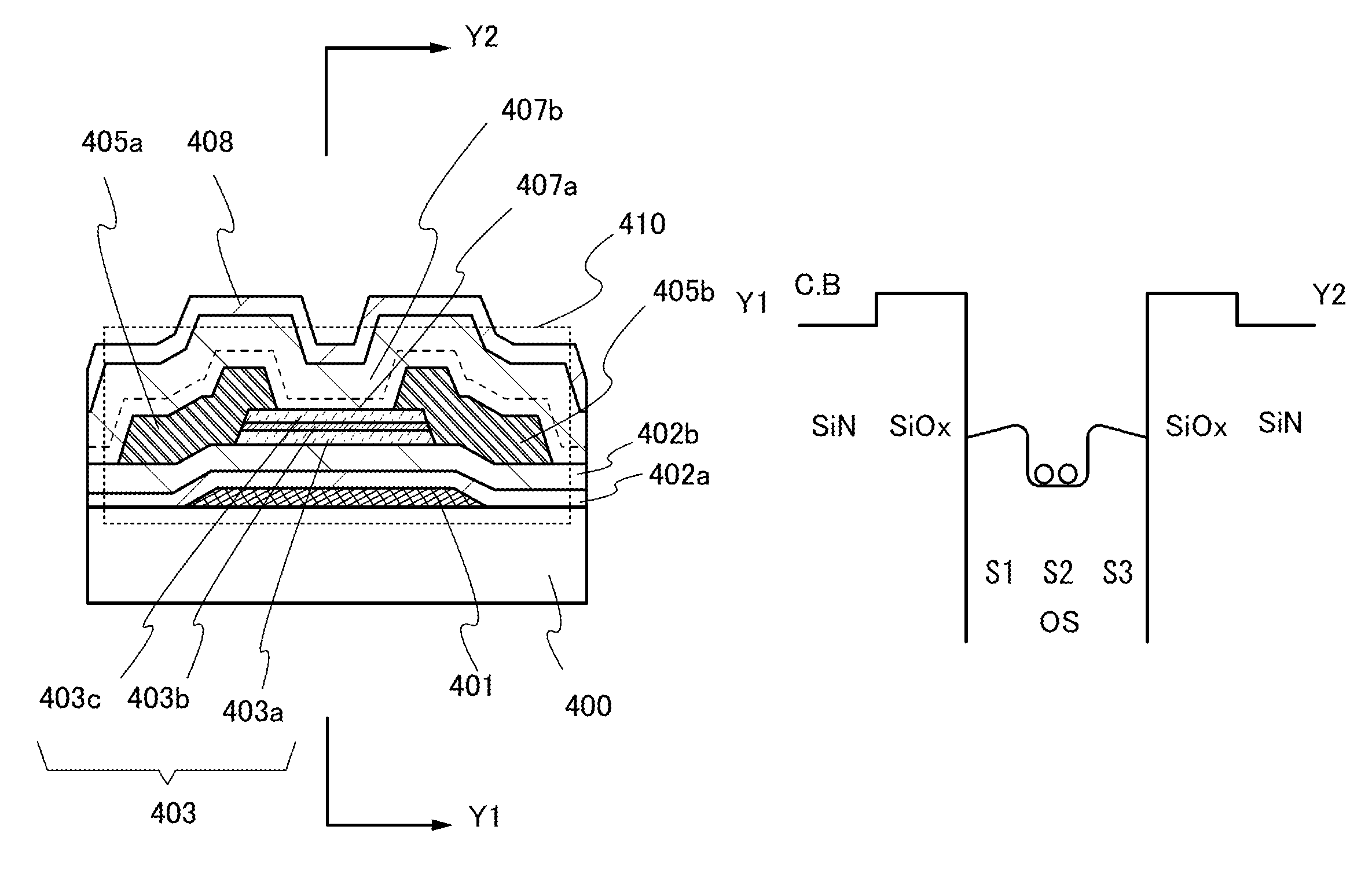
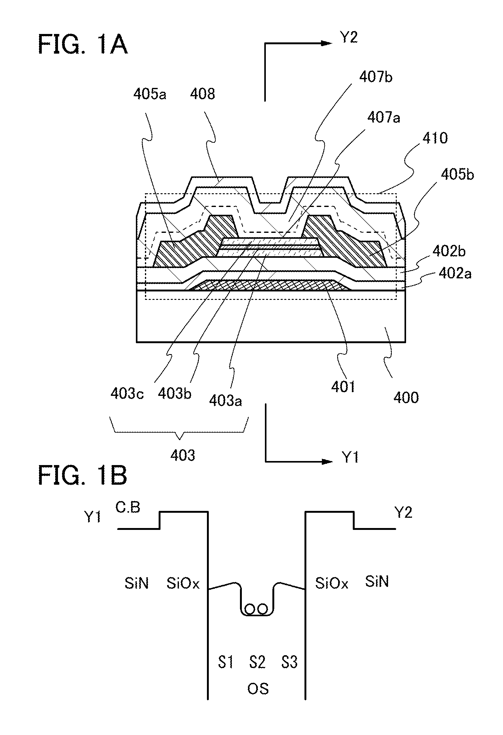
[0080]In this embodiment, one embodiment of a semiconductor device is described with reference to FIGS. 4A and 4B. In this embodiment, a transistor 311 including a first semiconductor material is provided in a lower portion, and a transistor 411 including a second semiconductor material is provided in an upper portion.

[0081]Here, the first semiconductor material and the second semiconductor material are preferably materials having different band gaps. For example, the first semiconductor material may be a semiconductor material other than an oxide semiconductor (e.g., silicon) and the second semiconductor material may be an oxide semiconductor. A transistor including a material such as silicon can easily operate at high speed. On the other hand, a transistor including an oxide semiconductor enables charge to be held for a long time owing to its characteristics.

[0082]As a substrate 300 used in the semiconductor device, a single crystal semiconductor substrate or a polycrystalline sem...

embodiment 2

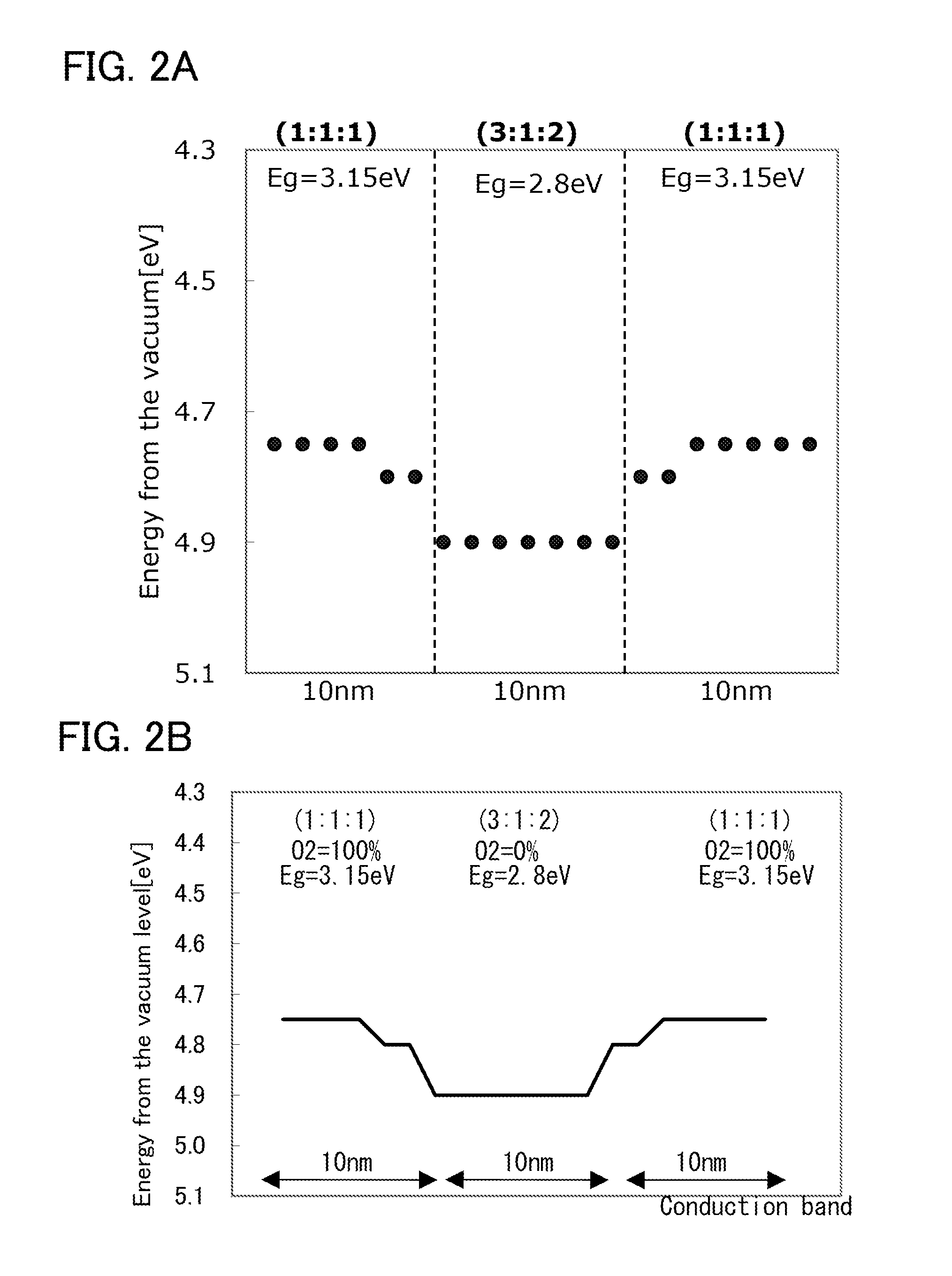
[0108]In this embodiment, an example which is partly different from Embodiment 1 is described below. The example of this embodiment differs from Embodiment 1 in the way to form the stack 403 of oxide semiconductor films, the way to supply oxygen, and the like.

[0109]The steps from formation of the transistor 311 using the first oxide semiconductor material in the lower portion up to formation of the second interlayer insulating film 308, the barrier layer 310, and the third wiring layer 309 are the same as those in Embodiment 1, and thus details of the steps are not described here.

[0110]A conductive film is formed over the barrier layer and selectively etched to form the fourth wiring layer 434 and the gate electrode 491.

[0111]Then, the insulating film 435 covering the gate electrode 491 is formed and planarized by CMP or the like. As the insulating film 435, an oxide insulating film containing nitrogen is used.

[0112]Then, the first gate insulating film 402a and the second gate insul...

embodiment 3

[0125]As another example of a semiconductor device including the transistor described in Embodiment 1 or 2, a circuit diagram of a NOR circuit, which is a logic circuit, is illustrated in FIG. 6A. FIG. 6B illustrates a circuit diagram of a NAND circuit.

[0126]In the NOR circuit illustrated in FIG. 6A, p-channel transistors 801 and 802 each have a structure similar to that of the transistor 311 in FIG. 4B in that a single crystal silicon substrate is used for a channel formation region, and n-channel transistors 803 and 804 each have a structure similar to that of the transistor 411 in FIG. 4B and that of the transistor 412 in FIG. 5 in that an oxide semiconductor film is used for a channel formation region.

[0127]In the NOR circuit in FIG. 6A, conductive layers controlling electrical characteristics of the transistors may be provided to overlap with gate electrode layers with oxide semiconductor films provided therebetween in the transistors 803 and 804. By controlling the potential o...


PUM


Abstract

A highly reliable semiconductor device exhibiting stable electrical characteristics is provided. Further, a highly reliable semiconductor device is provided. Oxide semiconductor films are stacked so that the conduction band has a well-shaped structure. A second oxide semiconductor film having a crystalline structure is provided over the first oxide semiconductor film and a third oxide semiconductor film is provided over the second oxide semiconductor film. The bottom of a conduction band in the second oxide semiconductor film is deeper from a vacuum level than the bottom of a conduction band in the first oxide semiconductor film and the bottom of a conduction band in the third oxide semiconductor film.

Description

BACKGROUND OF THE INVENTION[0001]1. Field of the Invention[0002]The present invention relates to a semiconductor device including an oxide semiconductor and a method for manufacturing the semiconductor device.[0003]In this specification, a semiconductor device generally means a device which can function by utilizing semiconductor characteristics, and an electrooptic device, a semiconductor circuit, and an electronic appliance are all semiconductor devices.[0004]2. Description of the Related Art[0005]In recent years, semiconductor devices have been developed to be used mainly for a CPU, or a memory. A CPU is an aggregation of semiconductor elements each provided with an electrode which is a connection terminal, which includes a semiconductor integrated circuit (including at least a transistor and a memory) separated from a semiconductor wafer.[0006]A semiconductor circuit (IC chip) of a CPU or a memory is mounted on a circuit board, for example, a printed wiring board, to be used as ...

Claims


Application Information

Patent Timeline
Patent Type & Authority Patents(United States)
IPC IPC(8): H01L29/792H01L21/8238H01L29/26H01L27/118H01L29/786
CPCH01L29/26H01L27/11807H01L29/7869H01L29/78696Y02E10/549H10K30/152
Inventor YAMAZAKI, SHUNPEI
Owner SEMICON ENERGY LAB CO LTD
Why Eureka
Try Eureka