

Semiconductor device and method for manufacturing the same
a technology of semiconductor devices and semiconductors, applied in the direction of semiconductor devices, electrical equipment, transistors, etc., can solve the problems of low reliability of semiconductor devices, and achieve the effects of stable electric characteristics, high reliability, and favorable dynamic characteristics
- Summary
- Abstract
- Description
- Claims
- Application Information
AI Technical Summary
Benefits of technology
Problems solved by technology
Method used
Image

Examples
embodiment 1
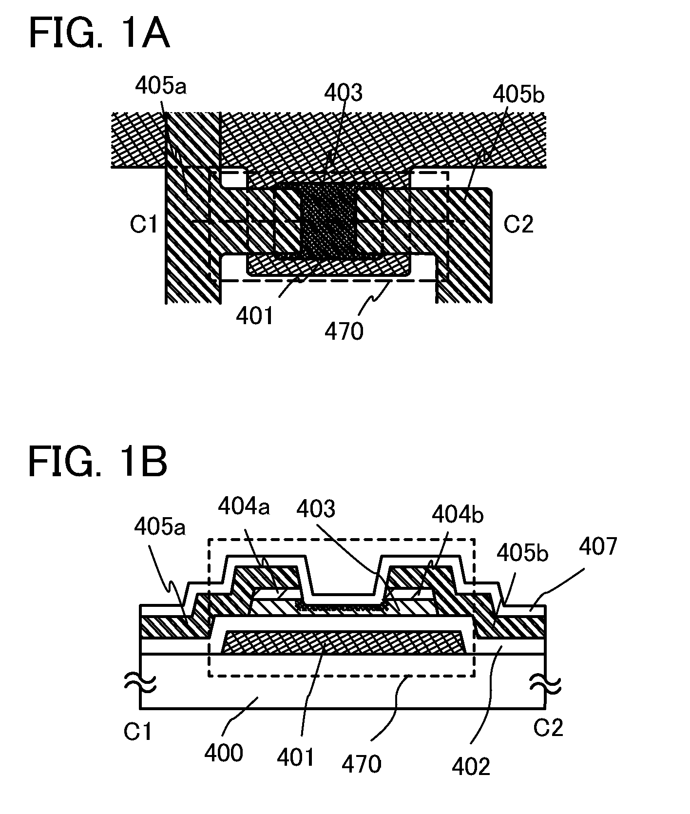
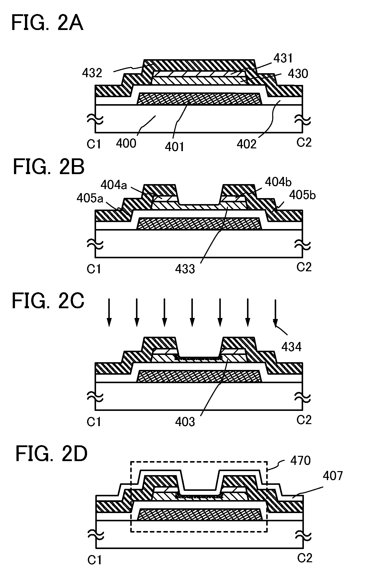
[0071]A semiconductor device and a method for manufacturing a semiconductor device will be described with reference to FIGS. 1A and 1B and FIGS. 2A to 2D.
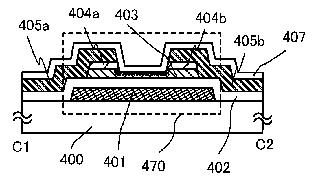
[0072]FIG. 1A is a top view of a thin film transistor 470 of a semiconductor device, and FIG. 1B is a cross-sectional view along line C1-C2 of FIG. 1A. The thin film transistor 470 is an inverted staggered thin film transistor and includes, over a substrate 400 which is a substrate having an insulating surface, a gate electrode layer 401, a gate insulating layer 402, a semiconductor layer 403, n+ layers 404a and 404b each serving as a source region or a drain region, and source or drain electrode layers 405a and 405b. In addition, an insulating film 407 is provided so as to cover the thin film transistor 470 and be in contact with the semiconductor layer 403.
[0073]The semiconductor layer 403 is an oxide semiconductor layer containing a metal element, to which at least one of metal elements of iron, nickel, cobalt, copper, gold, man...
embodiment 2
[0099]In this embodiment, FIGS. 30A to 30E illustrate an example of a semiconductor device including a thin film transistor in which a metal element is added to a semiconductor layer before formation of source and drain electrode layers, which is different from Embodiment 1.
[0100]FIGS. 30A to 30E are cross-sectional views illustrating a manufacturing process of a thin film transistor 440.
[0101]In FIG. 30A, a gate electrode layer 401 is formed over a substrate 400, and a gate insulating layer 402 is formed over the gate electrode layer 401.
[0102]A first oxide semiconductor film 435 is formed over the gate insulating layer 402.
[0103]Next, a metal element 434 is added to the first oxide semiconductor film 435, whereby a first oxide semiconductor film 436 is formed (FIG. 30B).
[0104]As the metal element 434, at least one of metal elements of iron, nickel, cobalt, copper, gold, manganese, molybdenum, tungsten, niobium, and tantalum can be used. For example, iron is used as the metal eleme...
embodiment 3
[0114]In this embodiment, FIGS. 31A to 31D illustrate an example of a semiconductor device including a thin film transistor in which source and drain electrode layers are in contact with a semiconductor layer without n+ layers interposed therebetween, which is different from Embodiment 1.
[0115]FIGS. 31A to 31D are cross-sectional views illustrating a manufacturing process of a thin film transistor 471.
[0116]In FIG. 31A, a gate electrode layer 401 is formed over a substrate 400, and a gate insulating layer 402 is formed over the gate electrode layer 401.
[0117]Over the gate insulating layer 402, a first oxide semiconductor film 430 is formed. The first oxide semiconductor film 430 is an island-shaped oxide semiconductor layer patterned by a photolithography step.
[0118]A conductive film 432 is formed over the gate insulating layer 402 and the first oxide semiconductor film 430.
[0119]The first oxide semiconductor film 430 and the conductive film 432 are etched by an etching step to form...
PUM
 Abstract
Description
Claims
Application Information