Semiconductor device including oxide semiconductor and metal oxide

a technology of metal oxide and semiconductor, applied in the direction of semiconductor devices, electrical equipment, transistors, etc., can solve the problems of potential electrical conductivity of oxide semiconductors, and achieve the effects of stable electrical characteristics, excellent electrical characteristics, and high reliability

Active Publication Date: 2014-11-04
SEMICON ENERGY LAB CO LTD
View PDF150 Cites 43 Cited by
  • Summary
  • Abstract
  • Description
  • Claims
  • Application Information

AI Technical Summary

Benefits of technology

[0007]In view of the above problem, an object is to provide a semiconductor device including an oxide semiconductor, which has stable electrical characteristics and improved reliability.
[0008]In one embodiment of the disclosed invention, insulating films each including a material containing a Group 13 element and oxygen are formed in contact with an oxide semiconductor film, whereby the interfaces with the oxide semiconductor film can be kept in a favorable state. Further, the insulating films each include a region where the proportion of oxygen is higher than that in the stoichiometric composition, so that oxygen is supplied to the oxide semiconductor film; thus, oxygen defects in the oxide semiconductor film can be reduced. Furthermore, the insulating films in contact with the oxide semiconductor film each have a stacked structure so that films each containing aluminum are provided over and under the oxide semiconductor film, whereby entry of water into the oxide semiconductor film can be prevented. Specifically, structures described below can be employed, for example.
[0017]According to one embodiment of the present invention, a transistor having stable electrical characteristics is provided.
[0018]Further, according to one embodiment of the present invention, a semiconductor device which includes a transistor having excellent electrical characteristics and high reliability can be provided.

Problems solved by technology

However, electrical conductivity of the oxide semiconductor may potentially change in the following case: the oxide semiconductor has deviation from the stoichiometric composition because of oxygen vacancy; a factor such as hydrogen or water causing formation of an electron donor enters the oxide semiconductor in a manufacturing process of a device; or the like.

Method used


Image

  • Semiconductor device including oxide semiconductor and metal oxide
  • Semiconductor device including oxide semiconductor and metal oxide
  • Semiconductor device including oxide semiconductor and metal oxide

Examples


embodiment 1

[Embodiment 1]

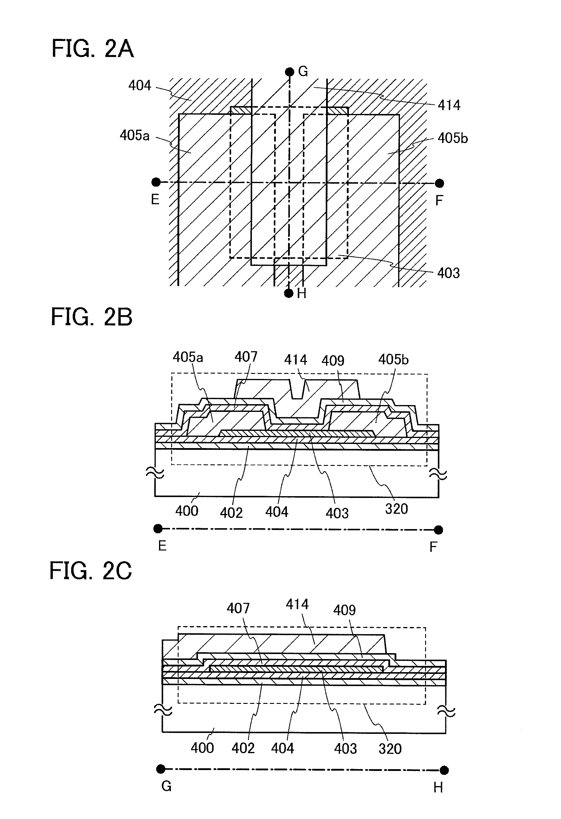
[0035]In this embodiment, one embodiment of a semiconductor device and a method for manufacturing the semiconductor device will be described with reference to FIGS. 1A to 1C, FIGS. 2A to 2C, FIGS. 3A to 3C, FIGS. 4A to 4F, FIGS. 5A to 5E, and FIGS. 6A to 6E.

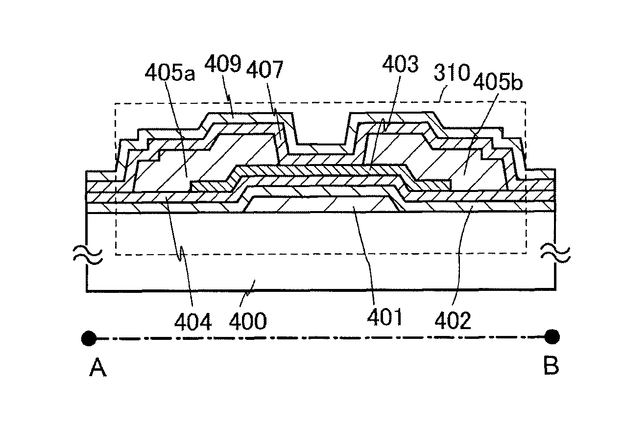
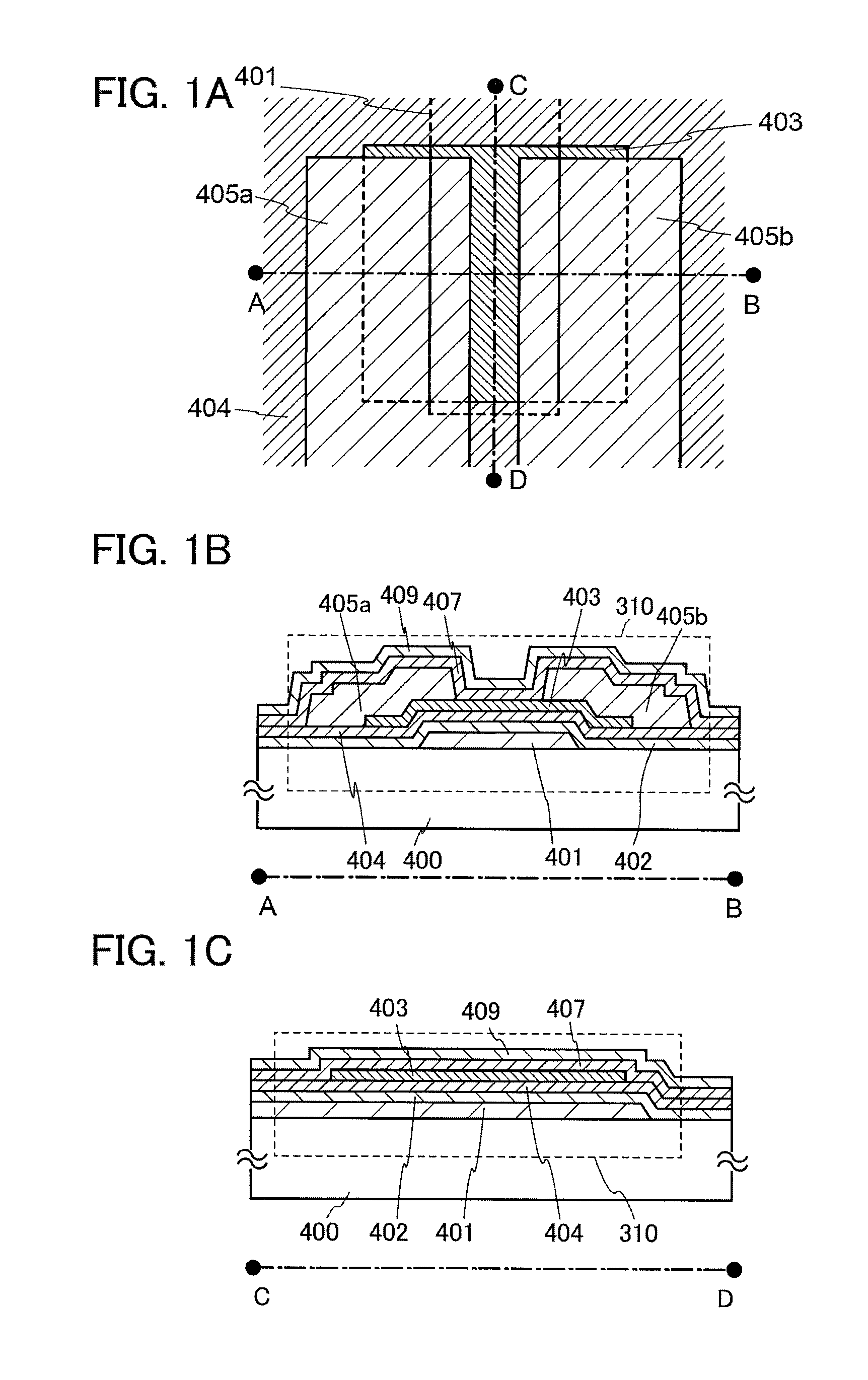
[0036]FIGS. 1A to 1C are a plan view and cross-sectional views of a transistor 310 as an example of a semiconductor device according to one embodiment of the disclosed invention. In FIGS. 1A to 1C, a bottom-gate transistor is illustrated as a transistor according to one embodiment of the disclosed invention. Here, FIG. 1A is a plan view and FIGS. 1B and 1C are cross-sectional views taken along line A-B and line C-D, respectively, of FIG. 1A. Note that part of components of the transistor 310 (e.g., a third metal oxide film 407, a fourth metal oxide film 409, and the like) is omitted in FIG. 1A for brevity.

[0037]The transistor 310 in FIGS. 1A to 1C includes, over a substrate 400 having an insulating surface, a gate e...

embodiment 2

[Embodiment 2]

[0144]A semiconductor device (also referred to as a display device) with a display function can be manufactured using the transistor an example of which is described in Embodiment 1. Moreover, some or all of the driver circuits which include the transistors can be formed over a substrate where the pixel portion is formed, whereby a system-on-panel can be obtained.

[0145]In FIG. 7A, a sealant 4005 is provided so as to surround a pixel portion 4002 provided over a first substrate 4001, and the pixel portion 4002 is sealed between the first substrate 4001 and a second substrate 4006. In FIG. 7A, a signal line driver circuit 4003 and a scan line driver circuit 4004 which are formed using a single crystal semiconductor film or a polycrystalline semiconductor film over a substrate separately prepared are mounted over the first substrate 4001, in a region that is different from the region surrounded by the sealant 4005. Various signals and potential are supplied to the signal ...

embodiment 3

[Embodiment 3]

[0228]A semiconductor device disclosed in this specification can be applied to a variety of electronic devices (including game machines). Examples of electronic devices are a television set (also referred to as a television or a television receiver), a monitor of a computer or the like, a camera such as a digital camera or a digital video camera, a digital photo frame, a mobile phone handset (also referred to as a mobile phone or a mobile phone device), a portable game machine, a portable information terminal, an audio reproducing device, a large-sized game machine such as a pachinko machine, and the like. Examples of electronic devices each including the liquid crystal display device described in the above embodiment are described.

[0229]FIG. 11A illustrates a laptop personal computer, which includes a main body 3001, a housing 3002, a display portion 3003, a keyboard 3004, and the like. By applying the semiconductor device described in Embodiment 1 or 2, the laptop pe...


PUM

PropertyMeasurementUnit
distanceaaaaaaaaaa
RF poweraaaaaaaaaa
temperatureaaaaaaaaaa

Abstract

An object is to provide a semiconductor device including an oxide semiconductor, which has stable electrical characteristics and improved reliability. In a transistor including an oxide semiconductor film, insulating films each including a material containing a Group 13 element and oxygen are formed in contact with the oxide semiconductor film, whereby the interfaces with the oxide semiconductor film can be kept in a favorable state. Further, the insulating films each include a region where the proportion of oxygen is higher than that in the stoichiometric composition, so that oxygen is supplied to the oxide semiconductor film; thus, oxygen defects in the oxide semiconductor film can be reduced. Furthermore, the insulating films in contact with the oxide semiconductor film each have a stacked structure so that films each containing aluminum are provided over and under the oxide semiconductor film, whereby entry of water into the oxide semiconductor film can be prevented.

Description

TECHNICAL FIELD[0001]The present invention relates to a semiconductor device and a method for manufacturing the semiconductor device.[0002]In this specification, a semiconductor device generally means a device which operates by utilizing semiconductor characteristics, and an electrooptic device, a semiconductor circuit, and electronic equipment are all semiconductor devices.BACKGROUND ART[0003]A technique by which transistors are formed using semiconductor thin films over a substrate having an insulating surface has been attracting attention. The transistor is applied to a wide range of electronic devices such as an integrated circuit (IC) and an image display device (display device). A silicon-based semiconductor material is widely known as a material for a semiconductor thin film applicable to a transistor. As another material, an oxide semiconductor has been attracting attention.[0004]For example, a transistor whose active layer uses an amorphous oxide containing indium (In), gal...

Claims


Application Information

Patent Timeline
Patent Type & Authority Patents(United States)
IPC IPC(8): H01L29/786H01L27/12H01L29/66H01L29/12
CPCH01L29/66742H01L27/1225H01L29/66969H01L29/7869H01L29/78606H01L29/78633H01L29/4908H01L29/51
Inventor YAMAZAKI, SHUNPEI
Owner SEMICON ENERGY LAB CO LTD
Why Eureka
Try Eureka