Semiconductor devices

a technology of semiconductor devices and semiconductor devices, applied in the direction of semiconductor devices, electrical equipment, transistors, etc., can solve the problems of inability to easily perform the process of forming air gaps in semiconductor devices having different densities of gate structures, and the method of effectively forming air gaps at the desired position has not been developed, so as to achieve stable electrical characteristics, reduce parasitic capacitance, and reduce resistance

Inactive Publication Date: 2012-01-12
SAMSUNG ELECTRONICS CO LTD
View PDF5 Cites 48 Cited by
  • Summary
  • Abstract
  • Description
  • Claims
  • Application Information

AI Technical Summary

Benefits of technology

[0070]According to example embodiments, a reaction prevention layer is formed on a portion of a sidewall of each of a plurality of gate structures spaced apart from each other, and a conductive layer is formed on portions of the gate structure that are not covered by the reaction prevention layer. The conductive layer may be reacted with the gate structures, e.g., by a heat treatment, to form a control gate having a low resistance. An insulation layer having an air gap between the gate structures may be formed by a process for forming a layer having low step coverage, so that the parasitic capacitance may be reduced. The air gap may be uniformly formed and may have a top surface higher than those of the gate structures.
[0071]Particularly, in a method of manufacturing a semiconductor device having different gate structure density at different regions, a mask may be formed on a sacrificial layer before removing the sacrificial layer and the insulation layer, and thus the sacrificial layer and the insulation layer may be prevented from being over-etched in a region having a low density of the gate structure by a loading effect. Thus, a control gate and a floating gate or a control gate and a source / drain region may be prevented from being electrically connected via a metal silicide layer, and the semiconductor device may have stable electrical characteristics.

Problems solved by technology

However, a method of forming an air gap effectively at a desired position has not been developed.
Particularly, a process for forming air gaps in a semiconductor device having different densities of gate structures is not easily performed.

Method used


Image

  • Semiconductor devices
  • Semiconductor devices
  • Semiconductor devices

Examples


Embodiment Construction

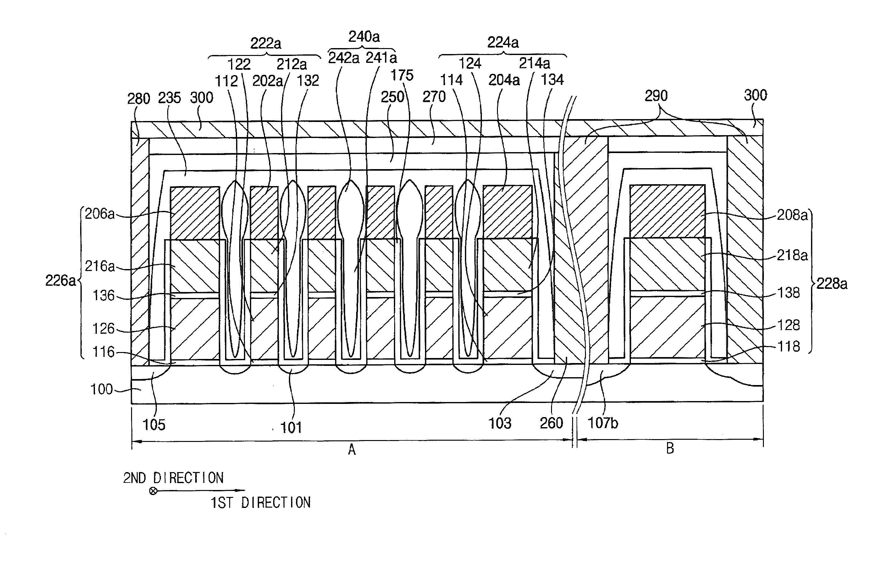
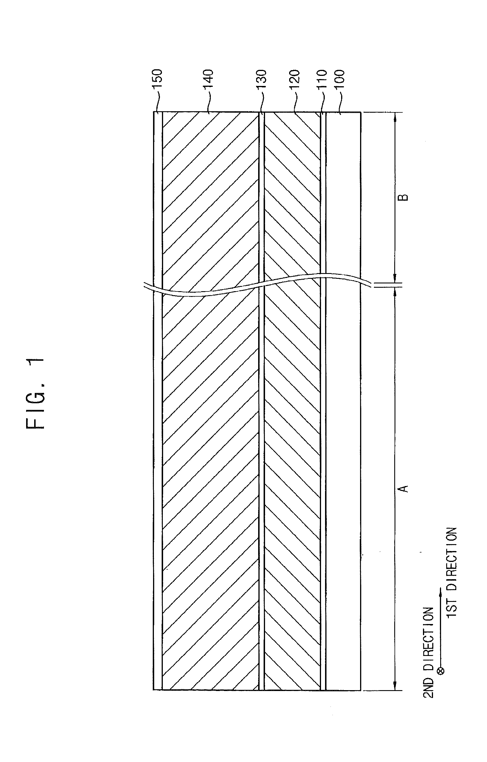
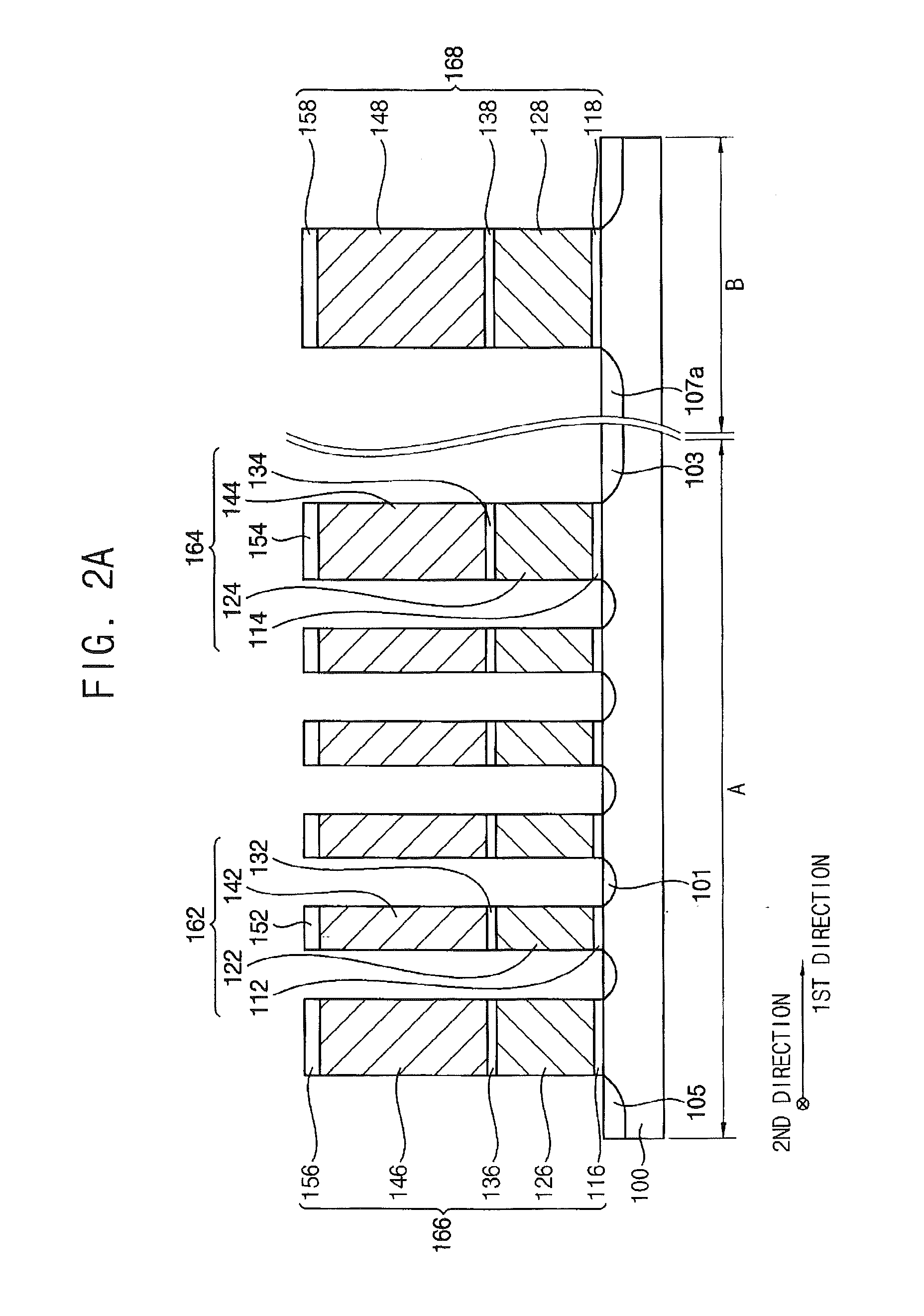
[0083]Various example embodiments will be described more fully hereinafter with reference to the accompanying drawings, in which some example embodiments are shown. The present inventive concept may, however, be embodied in many different forms and should not be construed as limited to the example embodiments set forth herein. Rather, these example embodiments are provided so that this description will be thorough and complete, and will fully convey the scope of the present inventive concept to those skilled in the art. In the drawings, the sizes and relative sizes of layers and regions may be exaggerated for clarity.

[0084]It will be understood that when an element or layer is referred to as being “on,”“connected to” or “coupled to” another element or layer, it can be directly on, connected or coupled to the other element or layer or intervening elements or layers may be present. In contrast, when an element is referred to as being “directly on,”“directly connected to” or “directly ...


PUM


Abstract

A semiconductor device includes a substrate, a plurality of gate structures, a first insulating interlayer pattern, and a second insulation layer pattern. The substrate has an active region and a field region, each of the active region and the field region extends in a first direction, and the active region and the field region are alternately and repeatedly arranged in a second direction substantially perpendicular to the first direction. The gate structures are spaced apart from each other in the first direction, each of the gate structures extends in the second direction. The first insulation layer pattern is formed on a portion of a sidewall of each gate structure. The second insulation layer pattern covers the gate structures and the first insulation layer pattern, and has an air tunnel between the gate structures, the air tunnel extending in the second direction.

Description

CLAIM OF PRIORITY[0001]This application claims priority under 35 USC § 119 to Korean Patent Application No. 10-2010-0066772 filed on Jul. 12, 2010 and No. 10-2010-0088199 filed on Sep. 9, 2010 in the Korean Intellectual Property Office (KIPO), the contents of which are herein incorporated by reference in their entirety.BACKGROUND[0002]1. Field[0003]Example embodiments relate to semiconductor devices and methods of manufacturing semiconductor devices. More particularly, example embodiments relate to semiconductor devices having air gaps and methods of manufacturing semiconductor devices having air gaps.[0004]2. Description of the Related Art[0005]As semiconductor devices have become more highly integrated, a threshold voltage may be changed due to the parasitic capacitance between word lines. Thus, a method of manufacturing a semiconductor device in which the parasitic capacitance may be reduced may be desired, and a method of forming an air gap between word lines has been developed....

Claims


Application Information

Patent Timeline
Patent Type & Authority Applications(United States)
IPC IPC(8): H01L29/788H01L27/088
CPCH01L21/28273H01L21/28282H01L21/764H01L27/11519H01L27/11526H01L27/11529H01L29/792H01L27/11573H01L29/42324H01L29/4234H01L29/66825H01L29/66833H01L29/7881H01L27/11565H01L29/40114H01L29/40117H10B41/10H10B41/40H10B41/41H10B43/10H10B43/40
Inventor LEE, MYOUNG-BUMSIM, JAE-HWANGPARK, IN-SUNHONG, JIN-GIGOO, JU-SEONPARK, SEUNG-BAELEE, SEUNG-YUPSONG, DU-HEONCHOE, JEONG-DONGLEE, SEOK-WON
Owner SAMSUNG ELECTRONICS CO LTD
Why Eureka
Try Eureka