

Semiconductor device
a technology of semiconductor devices and semiconductors, applied in semiconductor devices, instruments, electrical apparatus, etc., can solve the problems of low reliability of transistors including oxide semiconductors, and achieve the effect of high reliability
- Summary
- Abstract
- Description
- Claims
- Application Information
AI Technical Summary
Benefits of technology
Problems solved by technology
Method used
Image

Examples
embodiment 1
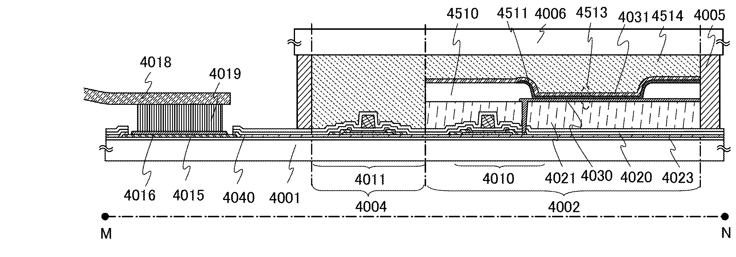
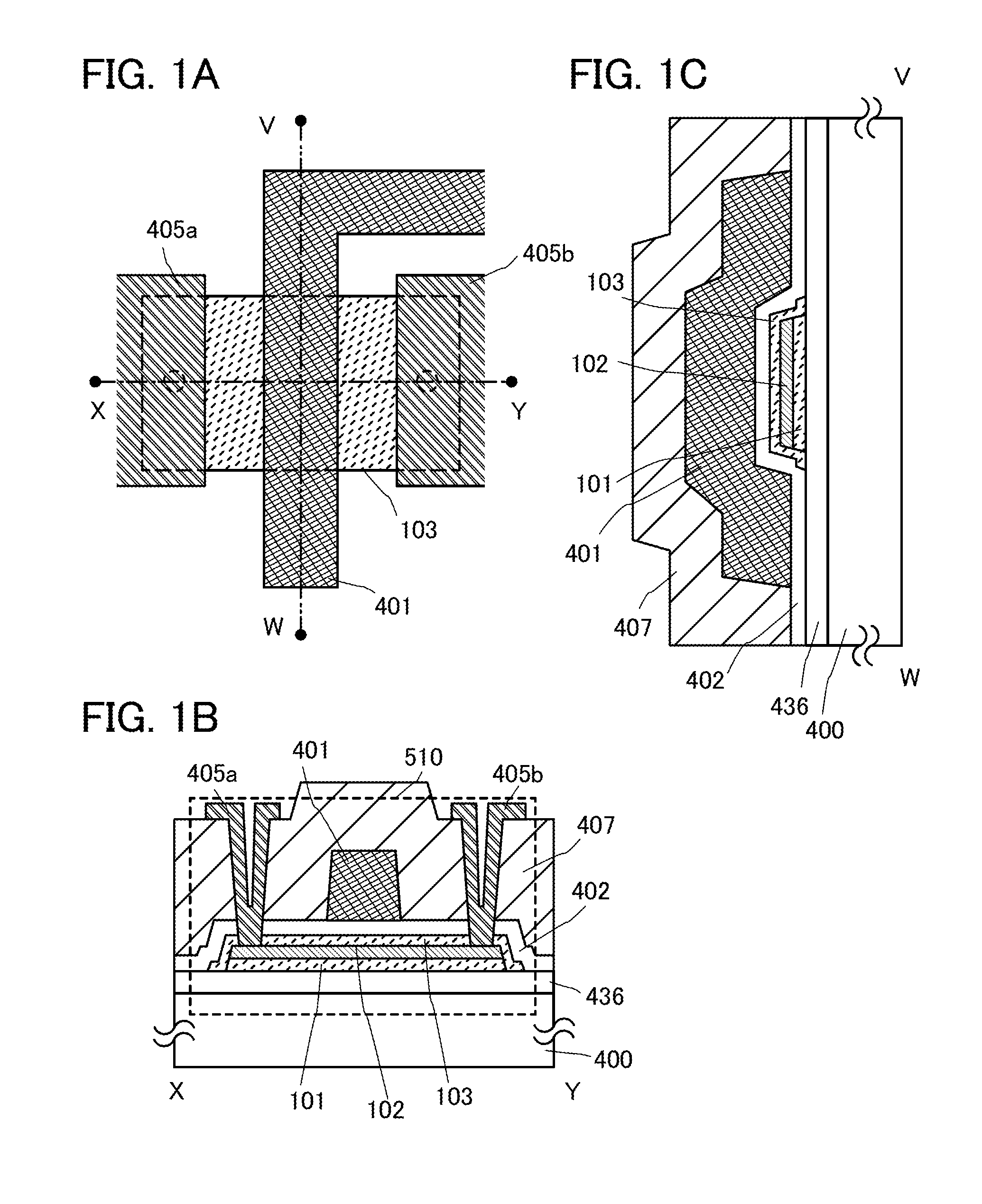
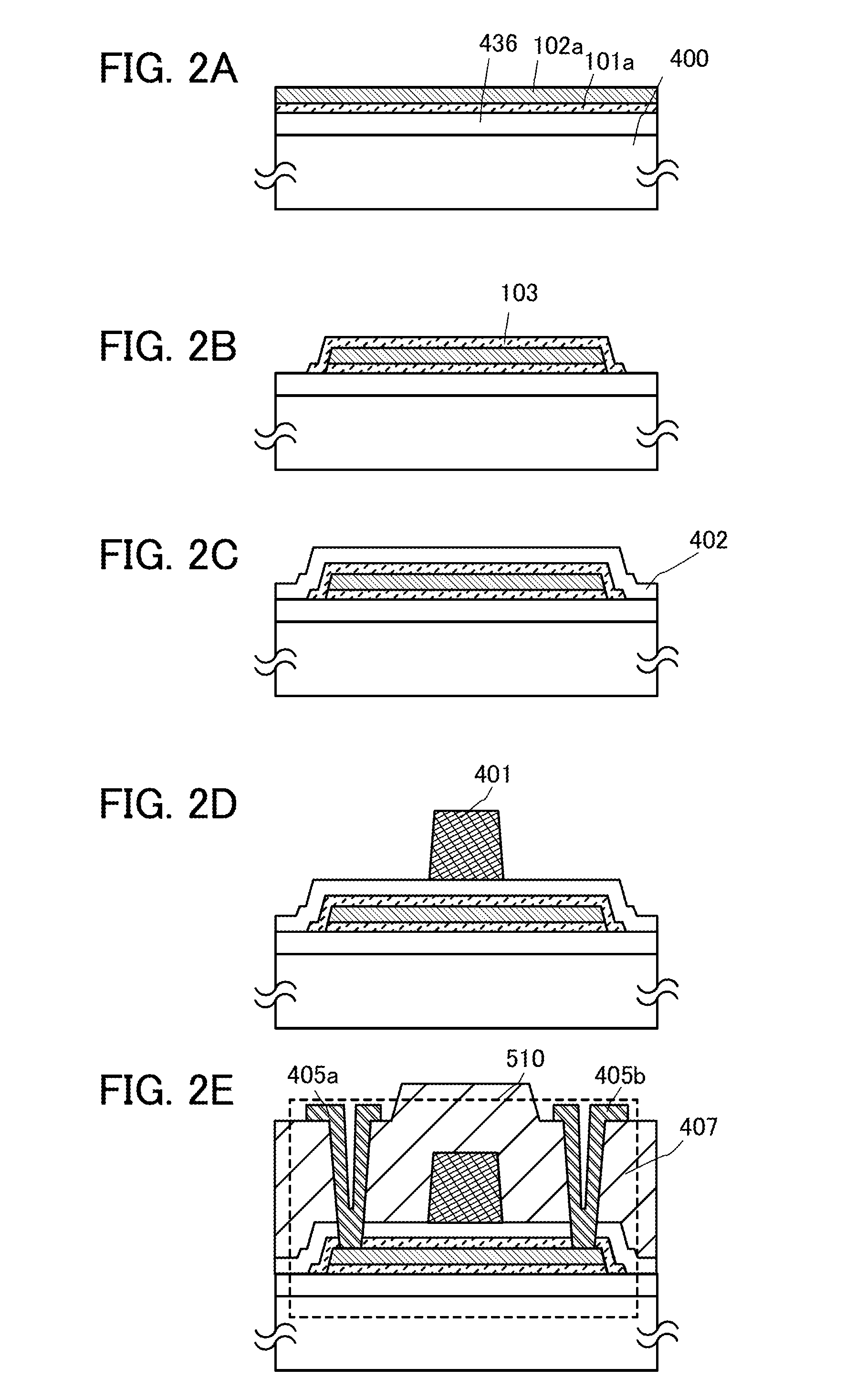
[0040]In this embodiment, one embodiment of a semiconductor device and a method of manufacturing the semiconductor device will be described with reference to FIGS. 1A to 1C, FIGS. 2A to 2E, and FIGS. 3A and 3B. In this embodiment, a transistor including an oxide semiconductor layer will be described as an example of the semiconductor device.
[0041]A transistor 510 illustrated in FIG. 1A, FIG. 1B, and FIG. 1C is an example of a top-gate transistor. FIG. 1A is a plan view, FIG. 1B is a cross-sectional view taken along chain line X-Y in FIG. 1A, and FIG. 1C is a cross-sectional view taken along chain line V-W in FIG. 1A.
[0042]As illustrated in FIG. 1B, which is a cross-sectional view in the channel length direction, the transistor 510 includes a first buffer layer 101, an oxide semiconductor layer 102, a second buffer layer 103, a gate insulating film 402, a gate electrode layer 401, an insulating film 407, a source electrode layer 405a, and a drain electrode layer 405b over a substrate...
embodiment 2
[0121]In this embodiment, another embodiment of a semiconductor device and a method of manufacturing the semiconductor device will be described with reference to FIGS. 5A to 5C. In this embodiment, the same portions as those in Embodiment 1 and portions having functions similar to those in Embodiment 1 and the same steps as those in Embodiment 1 and steps similar to those in Embodiment 1 may be handled as in Embodiment 1, and repeated description is omitted. In addition, detailed description of the same portions is not repeated.
[0122]This embodiment shows an example in which in a method of manufacturing a semiconductor device according to one embodiment of the disclosed invention, oxygen (including at least one of an oxygen radical, an oxygen atom, and an oxygen ion) is introduced into an oxide semiconductor layer that has been subjected to dehydration or dehydrogenation treatment so that oxygen is supplied to the oxide semiconductor layer.
[0123]Through the dehydration or dehydrogen...
embodiment 3
[0139]In this embodiment, another embodiment of a semiconductor device and a method of manufacturing the semiconductor device will be described with reference to FIGS. 6A to 6C. In this embodiment, the same portions as those in the above embodiment and portions having functions similar to those in the above embodiment and the same steps as those in the above embodiment and steps similar to those in the above embodiment may be handled as in the above embodiment, and repeated description is omitted. In addition, detailed description of the same portions is not repeated.
[0140]Described in this embodiment is an example in which low-resistance regions are formed in an oxide semiconductor layer in a method of manufacturing a semiconductor device according to one embodiment of the disclosed invention. The low-resistance regions can be formed by adding an impurity (also called a dopant) for changing the electrical conductivity to the oxide semiconductor layer.
[0141]As in the manufacturing p...
PUM
 Abstract
Description
Claims
Application Information