Semiconductor device and method for manufacturing the same

a semiconductor film and semiconductor technology, applied in the field of semiconductor films, can solve the problems of large amount of oxygen or hydrogen diffused, large amount of voids or distortions in the film, and easy interface reaction, and achieve the effect of improving reliability and reducing oxygen vacancies in the oxide semiconductor film

Active Publication Date: 2013-06-20
SEMICON ENERGY LAB CO LTD
View PDF2 Cites 42 Cited by
  • Summary
  • Abstract
  • Description
  • Claims
  • Application Information

AI Technical Summary

Benefits of technology

[0040]By increasing the temperature of the deposition-target substrate, migration of sputtering particles is likely to occur on a substrate surface. With this effect, a flat-plate-like sputtered particle reaches the substrate surface, moves slightly, and then is attached to the substrate surface with a flat plane (a-b plane) of the sputtered particle facing toward the substrate surface. Therefore, an oxide semiconductor film having a crystal region which is c-axis-aligned perpendicularly to the surface of the oxide semiconductor film is easily formed.
[0041]Further, heat treatment at a temperature of higher than or equal to 200° C. may be performed after the deposition of the oxide semiconductor film, so that a denser film is obtained. However, in that case, oxygen vacancies might be gen...

Problems solved by technology

For example, if an oxide semiconductor film having low film density is formed, the film tends to have a large number of voids or a large amount of distortion, whereby interface reaction occurs eas...

Method used


Image

  • Semiconductor device and method for manufacturing the same
  • Semiconductor device and method for manufacturing the same
  • Semiconductor device and method for manufacturing the same

Examples


embodiment 1

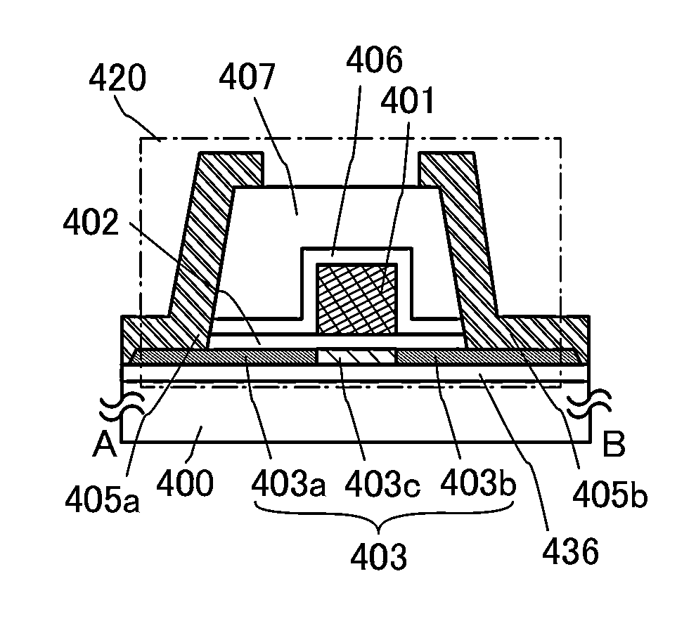
[0066]In this embodiment, one embodiment of a semiconductor device and a method of manufacturing the semiconductor device will be described with reference to FIG. 3A.

[0067]FIGS. 3A and 3B are a plan view and a cross-sectional view of a transistor 420 as one example of a semiconductor device. FIG. 3A is a plan view of the transistor 420 and FIG. 3B is a cross-sectional view taken along line A-B in FIG. 3A. Note that in FIG. 3A, part of components of the transistor 420 (e.g., an insulating layer 407) is omitted for simplicity.

[0068]The transistor 420 shown in FIGS. 3A and 3B includes a base insulating layer 436 provided over a substrate 400, an oxide semiconductor film 403 over the base insulating layer 436, a gate insulating layer 402 over the oxide semiconductor film 403, a gate electrode layer 401 provided over the oxide semiconductor film 403 with the gate insulating layer 402 provided therebetween, an insulating layer 406 and the insulating layer 407 which are provided over the g...

embodiment 2

[0136]In this embodiment, an example of a structure which is different from Embodiment 1 is described using FIGS. 3C and 3D. Portions which are the same as those in Embodiment 1 are denoted by the same reference numerals, and detail description thereof is skipped for simplicity.

[0137]FIG. 3C is a plan view of a transistor 421, and FIG. 3D is a cross-sectional view taken along line C-D in FIG. 3C. The transistor 421 illustrated in FIG. 3C includes a base insulating layer 436 provided over a substrate 400, an oxide semiconductor film 403 over the base insulating layer 436, a gate insulating layer 402 over the oxide semiconductor film 403, a gate electrode layer 401 provided over the oxide semiconductor film 403 with the gate insulating layer 402 provided therebetween, an insulating layer 406 and an insulating layer 407 which are provided over the gate electrode layer 401, a source electrode layer 405a and a drain electrode layer 405b which are electrically connected to the oxide semic...

embodiment 3

[0144]In this embodiment, an example of a structure which is different from Embodiment 1 is described using FIGS. 4A and 4B. Portions which are the same as those in Embodiment 1 are denoted by the same reference numerals, and detail description thereof is skipped for simplicity.

[0145]FIG. 4A is a plan view of a transistor 422, and FIG. 4B is a cross-sectional view taken along line E-F in FIG. 4A.

[0146]As illustrated in FIG. 4B that is the cross-sectional view in the channel length direction, the transistor 422 includes over a substrate 400 provided with a base insulating layer 436, an oxide semiconductor film 403 including a channel formation region 403c and low-resistance regions 403a and 403b, a source electrode layer 405a, a drain electrode layer 405b, a gate insulating layer 402, a gate electrode layer 401, sidewall insulating layers 412a and 412b provided on sides of the gate electrode layer 401, an insulating layer 413 provided over the gate electrode layer 401, an insulating ...


PUM


Abstract

To manufacture a highly reliable semiconductor device by giving stable electric characteristics to a transistor. An oxide semiconductor film is deposited by a sputtering method with the use of a polycrystalline sputtering target. In that case, partial pressure of water in a deposition chamber before or in the deposition is set to be lower than or equal to 10−3 Pa, preferably lower than or equal to 10−4 Pa, more preferably lower than or equal to 10−5 Pa. Thus, a dense oxide semiconductor film is obtained. The density of the oxide semiconductor film is higher than 6.0 g/cm3 and lower than 6.375 g/cm3.

Description

TECHNICAL FIELD[0001]The present invention relates to a semiconductor device including an oxide semiconductor and a manufacturing method thereof.[0002]In this specification, a semiconductor device generally means a device which can function by utilizing semiconductor characteristics, and an electrooptic device, a semiconductor circuit, and electronic equipment are all semiconductor devices.BACKGROUND ART[0003]Many transistors formed over a glass substrate or the like are manufactured using amorphous silicon, polycrystalline silicon, or the like, as typically seen in liquid crystal display devices. Although transistors including amorphous silicon have low field effect mobility, they can be formed over a larger glass substrate. On the other hand, although transistors including polycrystalline silicon have high field effect mobility, they are not suitable for being formed over a larger glass substrate.[0004]Other than a transistor formed using silicon, a technique in which a transistor...

Claims


Application Information

Patent Timeline
IPC IPC(8): H01L29/24H01L21/02
CPCH01L21/02565H01L29/247H01L21/02631H01L21/02554H01L27/1225H01L29/04H01L21/02422H01L29/7869H01L29/41733H01L29/78696H01L29/045H01L29/24H01L29/78606
Inventor YAMAZAKI, SHUNPEIAKIMOTO, KENGONONAKA, YUSUKEKANEMURA, HIROSHI
Owner SEMICON ENERGY LAB CO LTD
Why Eureka
Try Eureka