MVA LCD device and pixel circuit thereof

a liquid crystal display and pixel circuit technology, applied in non-linear optics, instruments, optics, etc., can solve the problems of narrow viewing angle, limited application of tn-lcd devices, and uneven distribution of va-lcd brightness, so as to improve narrow viewing angle and improve narrow viewing angle

Active Publication Date: 2010-07-27
AU OPTRONICS CORP
View PDF6 Cites 18 Cited by
  • Summary
  • Abstract
  • Description
  • Claims
  • Application Information

AI Technical Summary

Benefits of technology

[0015]The present invention provides a circuit of a pixel of a multi-domain vertical alignment liquid crystal display (MVA LCD) device. The circuit of a pixel of a MVA LCD device can improve the narrow viewing angle of the conventional MVA LCD device. The related MVA LCD device that can improve the narrow viewing angle of the conventional MVA LCD device is also provided.
[0016]The present invention also provides a circuit of a pixel of a MVA LCD device, which can improve the distribution of the brightness of the conventional MVA LCD device. The related MVA LCD device that can improve the distribution of the brightness of the conventional MVA LCD device is also provided.

Problems solved by technology

However, despite the related TN technologies improve a lot recently, the disadvantage of the TN-LCD devices such as narrow viewing angle still needs to be improved.
Moreover, the application of the TN-LCD device is also limited by the disadvantage of the narrow viewing angle.
However, the distribution of the brightness of the VA-LCD is not homogeneous, because each liquid crystal molecule has a character of the birefringence.
Hence, the distribution of the brightness of the conventional multi-domain vertical alignment liquid crystal display device is not homogeneous.
The display quality of the conventional multi-domain vertical alignment liquid crystal display device deteriorates, too.
However, in the above-mentioned Japan Patent Application Publications, the angular Gamma offset of all gray-tone still cannot be proved effectively.
Therefore, the MVA LCD provided by the above-mentioned Japan Patent Application Publications still encounter the problem of the non-homogeneous distribution of the brightness.

Method used


Image

  • MVA LCD device and pixel circuit thereof
  • MVA LCD device and pixel circuit thereof
  • MVA LCD device and pixel circuit thereof

Examples


embodiment 1

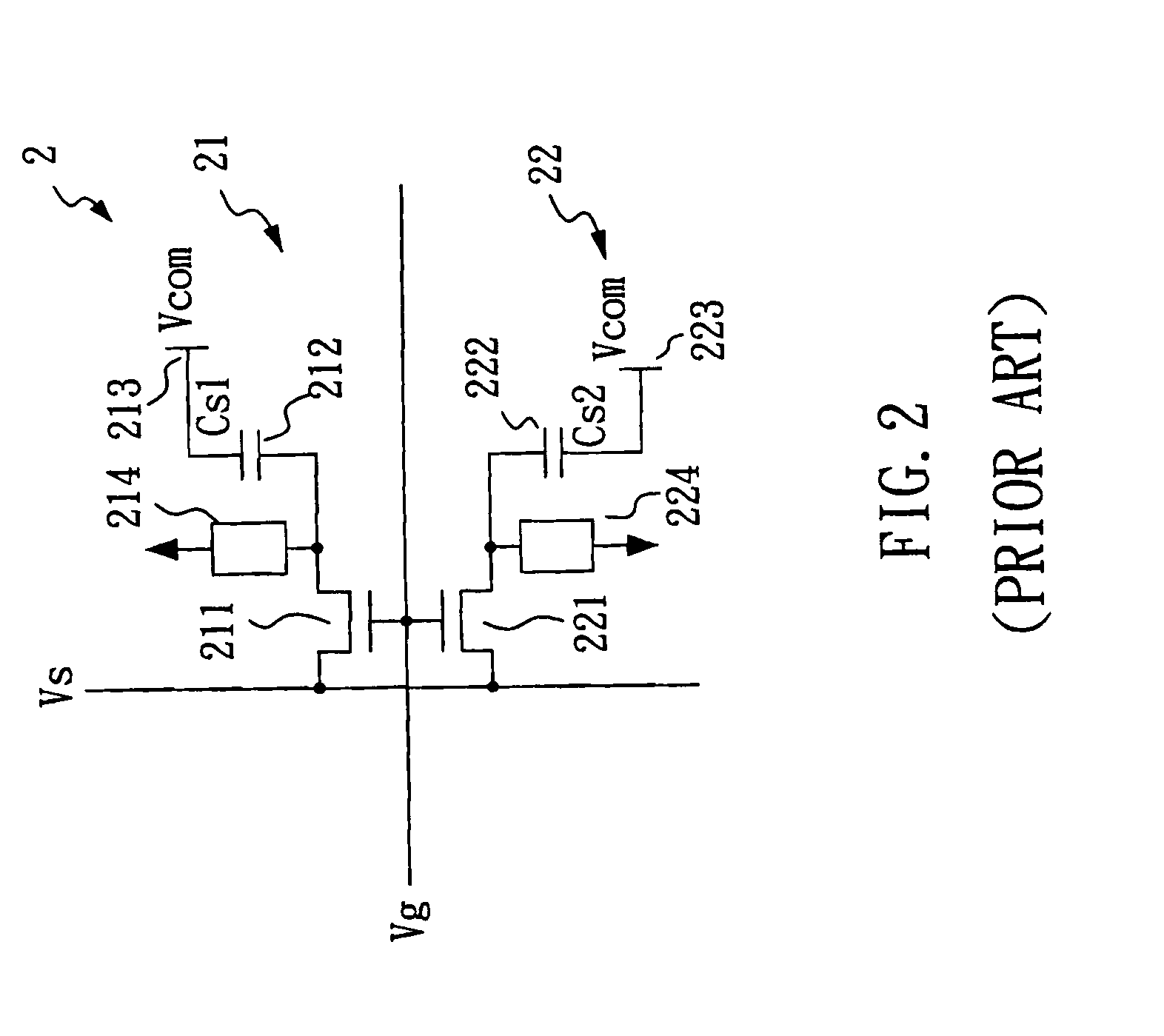
[0052]FIG. 3 is a scheme of the circuit of a pixel 3 of the multi-domain vertical alignment liquid crystal display (MVA LCD) device of the present invention. The pixel 3 of the multi-domain vertical alignment liquid crystal display device of the present invention comprises sub-pixel units 301, 302, a data line 31, a scan line (Vg) 32, a storage bus line (Vcom) 33, a coupling signal line (Vcs2) 34, thin film transistors 351, 352, liquid crystal capacitors 361, 362, and storage capacitors 371, 372.

[0053]The sources of the thin film transistors 351, 352 are electrically connected to the data line 31. The gates of the transistors 351, 352 are electrically connected to the scan line 32. The drains of the transistors 351, 352 are electrically connected to the terminals of the liquid crystal capacitors 361, 362, and the terminals of the storage capacitors 371, 372. The other terminal of the storage capacitor 371 is electrically connected to the coupling signal line 34. On the other hand, t...

embodiment 2

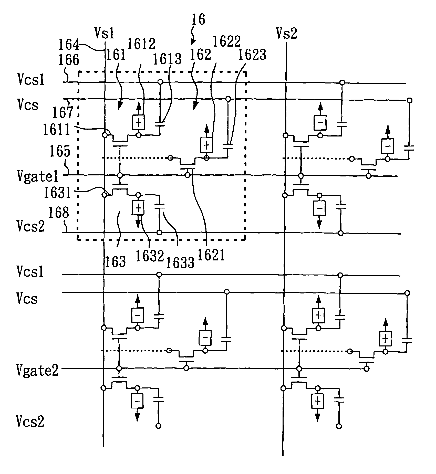
[0073]FIG. 14 is a schematic diagram of pixel circuits according to a preferred embodiment of the invention. In FIG. 14, a single pixel circuit 16 comprises sub-pixel units 161 to 163, a data line 164, a scan line (Vg) 165, a first coupling signal line (Vcs1) 166, a storage bus line 167 and a second coupling signal line (Vcs2) 168. The sub-pixel unit 161 comprises a TFT 1611, an LC capacitor 1612 and a storage capacitor 1613. The sub-pixel unit 162 comprises a TFT 1621, an LC capacitor 1622 and a storage capacitor 1623. The sub-pixel unit 163 comprises a TFT 1631, an LC capacitor 1632 and a storage capacitor 1633.

[0074]The data line 164 is electrically connected to the respective sources of the TFTs 1611, 1621, 1631. The scan line 165 is electrically connected to the respective gates of the TFTs 1611, 1621, 1631. In addition, the TFT 1611 comprises a drain electrically connected to one end of the LC capacitor 1612 and one end of the first storage capacitor 1613. The TFT 1621 compris...


PUM

PropertyMeasurementUnit
voltagesaaaaaaaaaa
pixel voltagesaaaaaaaaaa
pixel voltageaaaaaaaaaa

Abstract

A MVA LCD device and a pixel circuit thereof are disclosed. Each pixel is divided into a first sub-pixel unit and a second sub-pixel unit. One terminal of the storage capacitance of the first sub-pixel unit is electrically connected to a coupling signal line, which is used for providing a coupling electrode voltage. One terminal of the storage capacitance of the second sub-pixel unit is electrically connected to the storage bus line which is used for providing a common voltage. Therefore, the pixel voltage of the first sub-pixel unit is different from the pixel voltage of the second sub-pixel unit through controlling the different coupling electrode voltage.

Description

BACKGROUND OF THE INVENTION[0001]1. Field of the Invention[0002]The present invention relates to a pixel circuit of a liquid crystal display device, and, more particularly, to a pixel circuit of a multi-domain vertical alignment liquid crystal display device.[0003]2. Description of Related Art[0004]Currently, a mode most widely adopted for the TFT LCD is a normally-white mode that is implemented in a twisted nematic (TN) LCD. The technology of manufacturing the TN TFT LCD has outstandingly advanced in recent years. Contrast and color reproducibility provided by the TN TFT LCD have surpassed those offered by the CRT[0005]The color saturation of the TN-LCD device is better than that of the conventional display devices (e.g. the CRT display devices). However, despite the related TN technologies improve a lot recently, the disadvantage of the TN-LCD devices such as narrow viewing angle still needs to be improved. Moreover, the application of the TN-LCD device is also limited by the disa...

Claims


Application Information

Patent Timeline
Patent Type & Authority Patents(United States)
IPC IPC(8): G02F1/136G02F1/1343G02F1/1337
CPCG02F1/13624G02F1/133707G02F1/136213G02F2001/133742G02F2001/134345G02F1/133742G02F1/134345
Inventor LEE, SEOK-LYUL
Owner AU OPTRONICS CORP
Why Eureka
Try Eureka