Pixel structure and liquid crystal display panel

a liquid crystal display and pixel structure technology, applied in non-linear optics, instruments, optics, etc., can solve the problems of image producing color washout effect, color shift problem of mva or mha tft-lcd, etc., to prevent the aperture ratio of the pixel structure from being reduced, easy to adjust the area ratio of various sub-pixels, and low color shift

Inactive Publication Date: 2010-11-09
CHUNGHWA PICTURE TUBES LTD
View PDF10 Cites 2 Cited by
  • Summary
  • Abstract
  • Description
  • Claims
  • Application Information

AI Technical Summary

Benefits of technology

[0011]Accordingly, the present invention is directed to a pixel structure. A liquid crystal display (LCD) panel having the pixel structure has low color shift, and can easily adjust the area ratio of various sub-pixels and prevent the aperture ratio of the pixel structure from being reduced.
[0012]Accordingly, the present invention is also directed to an LCD panel for reducing color shift.
[0030]According to the pixel division design provided by the present invention, a pixel is divided into two or more sub-pixels, and an area ratio between a coupling capacitance, a storage capacitance, and a liquid crystal capacitance is adjusted by electrically connecting the drain electrode of the TFT to the primary pixel electrode and electrically coupling the drain electrode of the TFT to the secondary pixel electrode. Thus, different sub-pixels have different pixel voltage levels, so that color shift is reduced. Besides, the coupling capacitor can be easily adjusted through different design of the drain electrode's shape. Moreover, a drain electrode of special shape may be used for replacing the light-shielding layer on the color filter substrate for shielding those domains showing abnormal displays.

Problems solved by technology

However, the MVA or MHA TFT-LCD still has the problem in color shift.
In particular, the image will produce a color washout effect when the user looks at the image from a large viewing angle.

Method used


Image

  • Pixel structure and liquid crystal display panel
  • Pixel structure and liquid crystal display panel
  • Pixel structure and liquid crystal display panel

Examples


first embodiment

[0045]FIG. 4 is a top view of a pixel structure according to the present invention. Referring to FIG. 4, the pixel structure 400 is suitable for being disposed on a substrate 300. The pixel structure 400 includes a scan line 410, a data line 420, a thin film transistor (TFT) 430, a primary pixel electrode 440, and at least one secondary pixel electrode 450 (only one of which is illustrated). The scan line 410 and the data line 420 are disposed on the substrate 300. The TFT 430 is disposed on the substrate 300 and is electrically connected to the scan line 410 and the data line 420. The primary pixel electrode 440 is electrically connected to a drain electrode 432 of the TFT 430 through a contact hole 480. The secondary pixel electrode 450 is disposed above the drain electrode 432, and the drain electrode 432 is electrically coupled to the secondary pixel electrode 450.

[0046]Referring to FIG. 4, the pixel structure 400 may further include a common electrode 470 disposed on the substr...

second embodiment

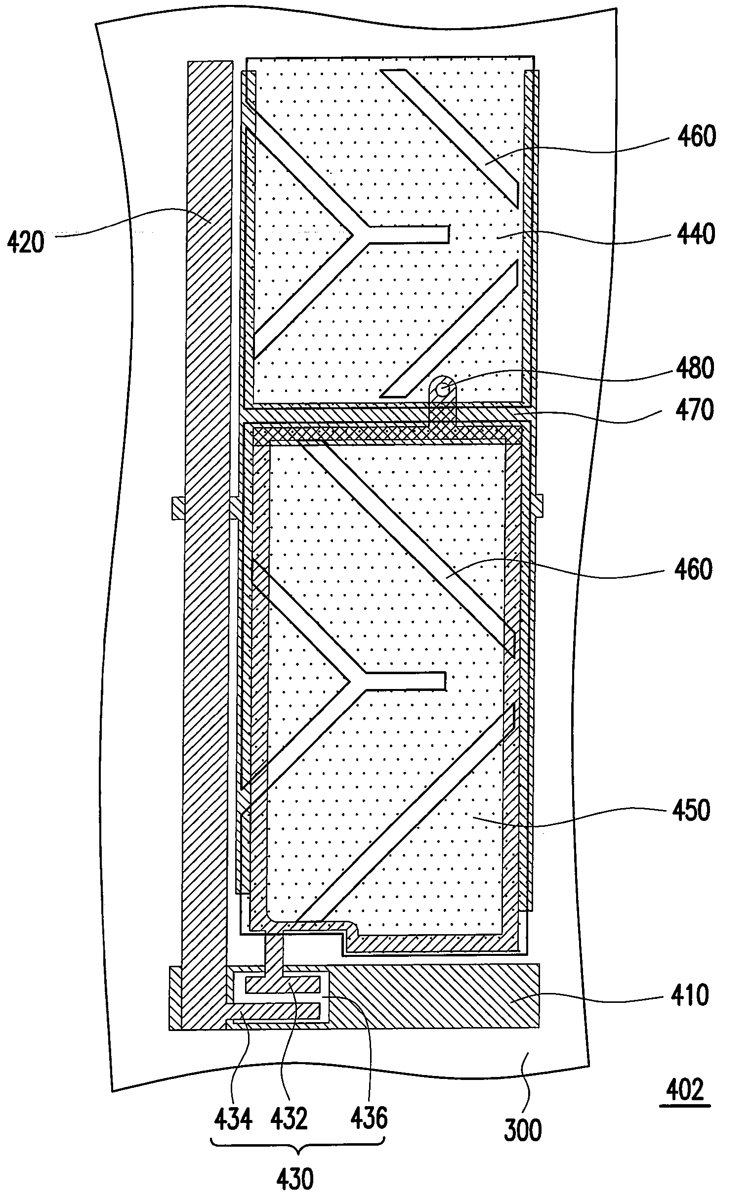
[0052]FIG. 5 is a top view of a pixel structure according to the present invention. Referring to FIG. 5, the pixel structure 402 is similar to the pixel structure 400 in FIG. 4, wherein like reference numerals refer to like components, and those similar components will not be described herein. It should be noted that in FIG. 5, the primary pixel electrode 440 and the secondary pixel electrode 450 have different areas.

[0053]Color shift can be further reduced by adjusting an area ratio of the primary pixel electrode 440 to the secondary pixel electrode 450. In particular, according to an embodiment of the present invention, an area ratio of the primary pixel electrode 440 to the secondary pixel electrode 450 in the pixel structures 400 and 402 is between 1:1 and 1:2. In addition, the primary pixel electrode 440 and the secondary pixel electrode 450 are independent of each other and are respectively disposed at two sides of the common electrode 470. Thus, compared to a conventional pix...

third embodiment

[0054]FIG. 6 is a top view of a pixel structure according to the present invention. Referring to FIG. 6, the pixel structure 404 is similar to the pixel structure 400 in FIG. 4, wherein like reference numerals refer to like components, therefore those similar components will not be described herein.

[0055]It should be noted here that in the present embodiment, the drain electrode 432 below the secondary pixel electrode 450 includes a main body 432a and an extension 432b. The main body 432a is disposed below one side of the secondary pixel electrode 450 and proximate to the scan line 410. The extension 432b is extended from the main body 432a to the primary pixel electrode 440 and is electrically connected to the primary pixel electrode 440.

[0056]Similarly, the drain electrode 432 of the TFT 430 is electrically coupled to the secondary pixel electrode 450, and the extension 432b of the drain electrode 432 is electrically connected to the primary pixel electrode 440 through the contact...


PUM

PropertyMeasurementUnit
area ratioaaaaaaaaaa
pixel structureaaaaaaaaaa
color shiftaaaaaaaaaa

Abstract

A pixel structure suitable for being disposed on a substrate is provided. The pixel structure includes a scan line, a data line, a thin film transistor (TFT), a primary pixel electrode, and at least one secondary pixel electrode. The scan line and the data line are disposed on the substrate. The TFT is disposed on the substrate and is electrically connected to the scan line and the data line. The primary pixel electrode is electrically connected to a drain electrode of the TFT through a contact hole. The secondary pixel electrode is disposed above the drain electrode and the drain electrode is electrically coupled to the secondary pixel electrode. Besides, a liquid crystal display (LCD) panel having the pixel structure is also provided.

Description

CROSS-REFERENCE TO RELATED APPLICATION[0001]This application claims the priority benefit of Taiwan application serial no. 96102845, filed Jan. 25, 2007. All disclosure of the Taiwan application is incorporated herein by reference.BACKGROUND OF THE INVENTION[0002]1. Field of the Invention[0003]The present invention relates to a pixel structure and a liquid crystal display (LCD) panel having the pixel structure. More particularly, the present invention relates to an LCD panel with low color shift and a pixel structure thereof.[0004]2. Description of Related Art[0005]Thin film transistor liquid crystal display (TFT-LCD) has become the mainstream in display market for it having such advantages as high image quality, high space efficiency, low power consumption, and no radiation etc. Presently, the performance of an LCD is proceeding towards high contrast ratio, rapid response, and wide viewing angle, wherein a multi-domain vertically alignment (MVA) TFT-LCD and a multi-domain horizontal...

Claims


Application Information

Patent Timeline
Patent Type & Authority Patents(United States)
IPC IPC(8): G02F1/1343
CPCG02F1/133753G02F1/134336G02F1/136286G02F2001/134345G02F1/134345
Inventor LIU, CHIH-CHUNGWANG, MING-TSUNGCHANG, YUEH-PING
Owner CHUNGHWA PICTURE TUBES LTD
Why Eureka
Try Eureka