Plasma display panel driving method

a plasma display panel and drive method technology, applied in the direction of gas discharge vessels/containers, electric discharge tubes, instruments, etc., can solve the problems of low image contrast, inability to provide dark images with high image quality, etc., to prevent erroneous discharge, low luminance, and differences in luminance

Inactive Publication Date: 2010-12-07
PANASONIC CORP
View PDF7 Cites 0 Cited by
  • Summary
  • Abstract
  • Description
  • Claims
  • Application Information

AI Technical Summary

Benefits of technology

[0010]An object of the present invention is to provide a driving method of a plasma display panel capable of enhancing the ability to express luminance contrast when displaying dark images.
[0014]Here, in the microemission step, potentials lower than the voltage generated between ones of the row electrodes and the others of row electrodes during application of a sustain pulse while applying a voltage as described above between ones of the row electrodes and the column electrodes, are respectively applied to the ones of the row electrodes and the others of the row electrodes so as to prevent erroneous discharge between each of the row electrodes serving as row electrode pairs.
[0015]Accordingly, according to this form of driving, since a microemission discharge having a low emission luminance accompanying a sustain discharge in comparison with that sustain discharge can be reliably generated, differences in luminance between each gradation expressing low luminance can be minimized, thereby enhancing the ability to express luminance contrast when expressing dark images.

Problems solved by technology

Here, since the reset discharge is a comparatively strong discharge and is not involved in any manner with the contents of the image to be displayed, there was the problem of luminescence accompanying this discharge lowering image contrast.
However, since it is not possible to adequately enhance so-called black contrast when displaying dark images even by using a driving method like that described above, there was the problem of being unable to provide dark images with high image quality.

Method used


Image

  • Plasma display panel driving method
  • Plasma display panel driving method
  • Plasma display panel driving method

Examples


Embodiment Construction

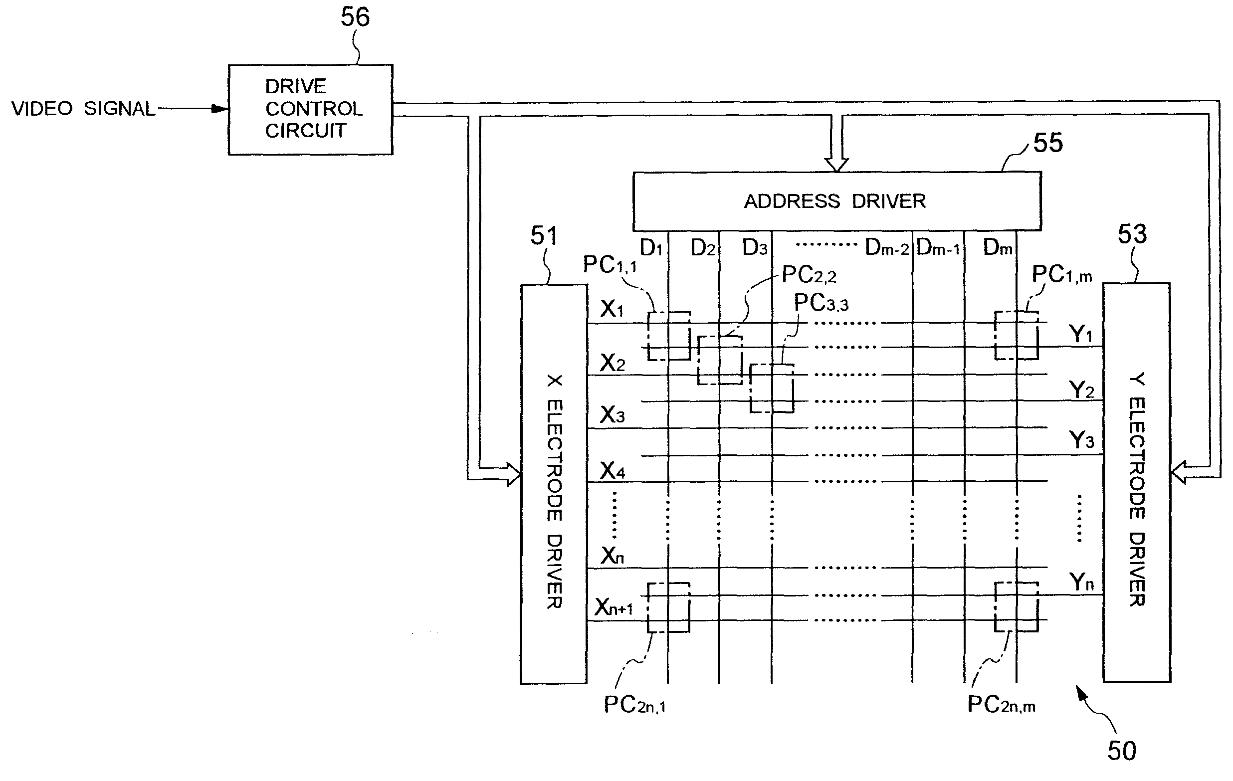
[0031]FIG. 1 schematically shows the constitution of a plasma display device in which a plasma display panel is driven according to the driving method according to the present invention.

[0032]As shown in FIG. 1, this plasma display device is composed of a plasma display panel in the form of a PDP 50, an X electrode driver 51, a Y electrode driver 53, an address driver 55, and a driving control circuit 56.

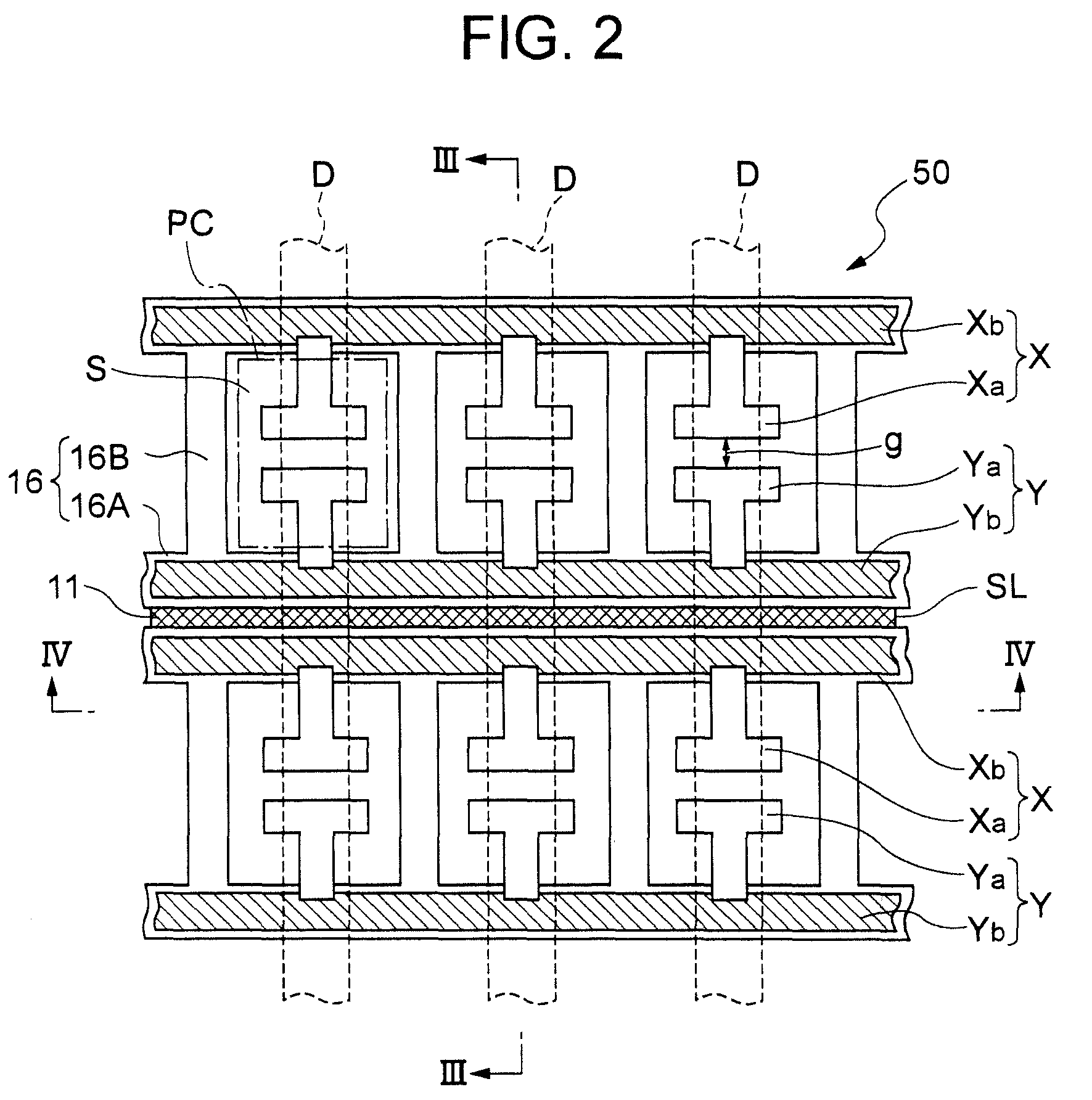
[0033]Column electrodes D1 to Dm each arranged extending in the longitudinal direction (vertical direction) of a two-dimensional display screen, and row electrodes X1 to Xn and row electrodes Y1 to Yn, each arranged extending in the lateral direction (horizontal direction), are formed in the PDP 50. Row electrode pairs forming a pair with mutually adjacent row electrodes (Y1,X1), (Y2,X2), (Y3,X3), . . . (Yn,Xn) respectively serve as a first display line to an nth display line in the PDP 50. A discharge cell (display cell) PC serving as a pixel is formed at the respective intersectio...


PUM


Abstract

A plasma display panel driving method in which a reset step and an address step are sequentially executed in the first subfield and second subfield of each field. A microemission step is executed in the first subfield for generating a microemission discharge between ones of the row electrodes and the column electrodes in display cells in the ON mode by applying a voltage for using the ones of the row electrodes as the anode and the column electrodes as the cathode, between the electrodes immediately after the address step. Moreover, in the microemission step, a potential lower than the voltage generated when applying a sustain pulse is respectively applied to the ones and the others of the row electrodes while applying a voltage as described above between the ones of the row electrodes and the column electrodes.

Description

BACKGROUND OF THE INVENTION[0001]1. Field of the Invention[0002]The present invention relates to a method for driving a plasma display panel.[0003]2. Description of the Related Art[0004]AC (alternating current) plasma display panels (to be referred to as PDP) are currently commercially available for use as thin display devices. A PDP houses two substrates consisting of a front transparent substrate and a rear substrate arranged in mutual opposition and separated by a predetermined gap. A plurality of row electrode pairs mutually forming pairs and respectively extending in the horizontal direction of the screen are formed on the inner surface of the front transparent substrate (surface opposing the rear substrate) serving as the display surface. Moreover, a dielectric layer covering each row electrode pair is formed on the inner surface of the front transparent substrate. A plurality of column electrodes extending in the vertical direction of the screen so as to intersect the row ele...

Claims


Application Information

Patent Timeline
Patent Type & Authority Patents(United States)
IPC IPC(8): G09G3/28H01J11/42G09G3/20G09G3/288G09G3/291G09G3/292G09G3/294G09G3/298H01J11/22H01J11/24H01J11/34H01J11/40
CPCG09G3/2927G09G3/2937G09G2310/066
Inventor ITAKURA, SHUNSUKETOKUNAGA, TSUTOMU
Owner PANASONIC CORP
Why Eureka
Try Eureka