Method of precharging local input/output line and semiconductor memory device using the method

a local input/output line and memory device technology, applied in the direction of information storage, static storage, digital storage, etc., can solve the problems of data not being accessed through dummy bit lines on the left, unnecessary power consumption, and the semiconductor memory device b>100/b> cannot operate normally during the read or write operation, so as to prevent excessive power consumption and abnormal operation

Inactive Publication Date: 2011-01-18
SAMSUNG ELECTRONICS CO LTD
View PDF9 Cites 0 Cited by
  • Summary
  • Abstract
  • Description
  • Claims
  • Application Information

AI Technical Summary

Benefits of technology

The present invention may provide a semiconductor memory device capable of precharging a local input / output line that is coupled to bit lines for inputting / outputting data and does not transmit data so as to prevent excessive power consumption and an abnormal operation.

Problems solved by technology

For example, when data of the memory cell array block MCB_1 is accessed, data is accessed through bit lines on the right; however, data cannot be accessed through dummy bit lines on the left.
As a result, when a write command or a read command is continuously performed to write or read data to or from the memory cell array blocks MCB_1 and MCB_k, the local input / output lines LIO_1, LIO_2L, LIO_k−1R, LIO_kL, LIO_kR, and LIO_k+1L are continuously precharged, thereby causing unnecessary power consumption.
As a result, the semiconductor memory device 100 can not operate normally during the read or write operation.

Method used


Image

  • Method of precharging local input/output line and semiconductor memory device using the method
  • Method of precharging local input/output line and semiconductor memory device using the method
  • Method of precharging local input/output line and semiconductor memory device using the method

Examples


Embodiment Construction

The attached drawings for illustrating exemplary embodiments of the present invention are referred to in order to gain a sufficient understanding of the present invention, the merits thereof, and the objectives accomplished by the implementation of the present invention.

Hereinafter, exemplary embodiments of the present invention will be described in detail with reference to the attached drawings. Like reference numerals in the drawings denote like elements.

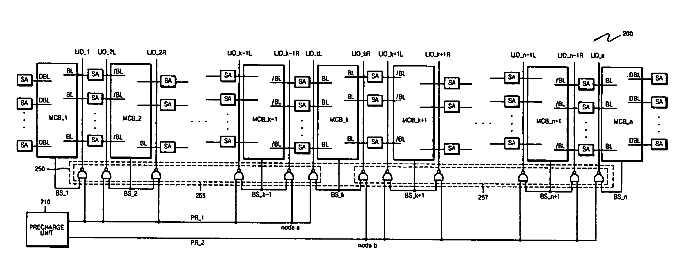
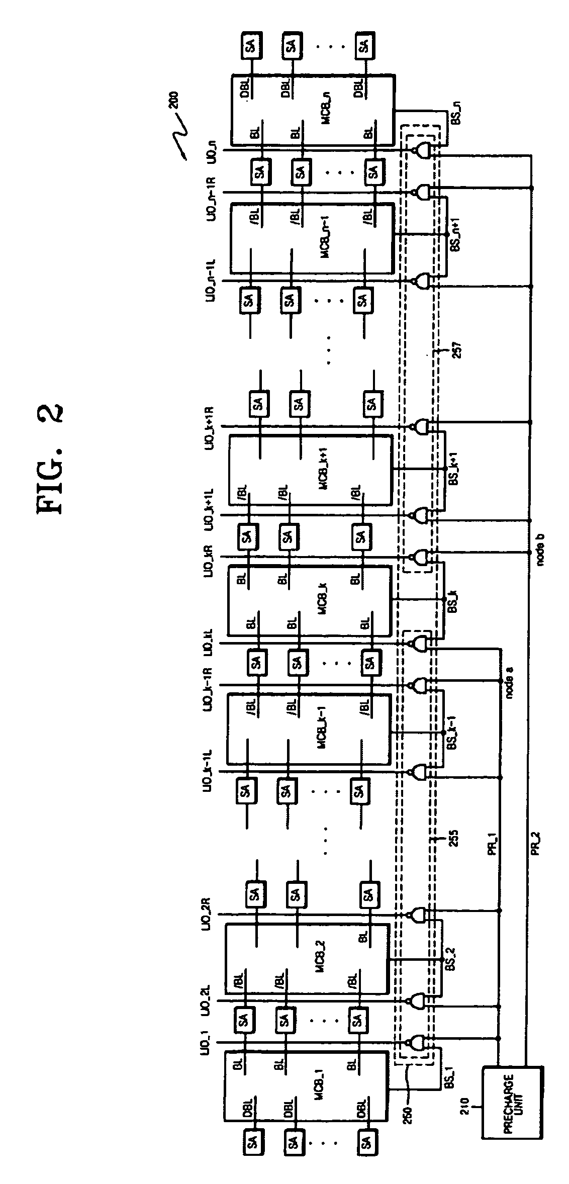
FIG. 2 is a block diagram illustrating a semiconductor memory device 200 according to an embodiment of the present invention. Referring to FIG. 2, the semiconductor memory device 200 may include first to n-th memory cell array blocks MCB_1 to MCB_n, a precharge unit 210, and a controller 250. The semiconductor memory device 200 includes a plurality of local input / output lines LIO_1, LIO_2L, LIO_2R, . . . , and LIO_n, and each local input / output line is coupled with bit lines BL of a corresponding memory cell array block to transmi...


PUM


Abstract

A method and semiconductor memory device for precharging a local input / output line. The semiconductor memory device, which may have an open bit line structure, transmits data through local input / output lines that are coupled to bit lines of first to n-th memory cell array blocks (n being a natural number). The semiconductor memory device may include a precharge unit configured to generate a plurality of precharge signals and a controller configured to control precharging of the at least one local input / output line responsive to block information corresponding to activation of at least one of the memory cell array blocks and responsive to at least one of the precharge signals.

Description

CROSS-REFERENCE TO RELATED PATENT APPLICATIONThis application claims the benefit of Korean Patent Application No. 10-2007-0079784, filed on Aug. 8, 2007, in the Korean Intellectual Property Office, the disclosure of which is incorporated herein in its entirety by reference.BACKGROUND OF THE INVENTION1. Field of the InventionThe present invention relates to a semiconductor memory device, and more particularly, to a method of precharging a local input / output line and a semiconductor memory device using the method.2. Description of the Related ArtA semiconductor memory device includes a plurality of cells to store data. The cells are divided into memory cell array blocks having a predetermined number of the cells. The cells that are arrayed in corresponding blocks are divided into banks to be arrayed.In the memory cell array blocks, memory cells are arrayed in units of a matrix. A plurality of word lines and a plurality of bit lines intersect with each other. In order to access data, a...

Claims


Application Information

Patent Timeline
Patent Type & Authority Patents(United States)
IPC IPC(8): G11C7/00
CPCG11C7/1048G11C8/18G11C7/12G11C11/4074G11C11/4096
Inventor KIM, MYEONG-OKIM, BYUNG-CHULCHU, YONG-GYU
Owner SAMSUNG ELECTRONICS CO LTD
Why Eureka
Try Eureka