Lead pin for package boards

a technology of lead pins and package boards, applied in the direction of final product manufacturing, sustainable manufacturing/processing, semiconductor/solid-state device details, etc., can solve the problems of solder paste, voids, and bubbles in solder

Inactive Publication Date: 2011-02-22
SAMSUNG ELECTRO MECHANICS CO LTD
View PDF6 Cites 11 Cited by
  • Summary
  • Abstract
  • Description
  • Claims
  • Application Information

AI Technical Summary

Benefits of technology

[0013]An advantage of the present invention is that it provides a lead pin for package boards, which includes a disk-shaped head having a hexagonal vertical cross-section or a cylindrical head having a plurality of grooves formed on the upper and lower surfaces thereof and a connection pin projecting from the center of the upper surface of the head.
[0014]Additional aspect and advantages of the present general inventive concept will be set forth in part in the description which follows and, in part, will be obvious from the description, or may be learned by practice of the general inventive concept.
[0015]According to an aspect of the invention, a lead pin for package boards comprises a disk-shaped head of which the diameter increases toward the middle portion thereof and that has a hexagonal vertical cross-sectional shape; and a connection pin that is formed so as to project from the center of the upper surface of the head.
[0016]The middle portion of the head may be formed to have a larger diameter than the upper and lower surfaces of the head.
[0017]The middle portion of the head may be formed to have a larger diameter than the connection pin.
[0018]According to another aspect of the invention, a lead pin for package board comprises a cylindrical head having a plurality of grooves formed on the upper and lower surfaces thereof, respectively; and a connection pin projecting from the center of the upper surface of the head.

Problems solved by technology

In this case, however, when the lead pin 13 is mounted, buoyancy may occur because an amount and state of the solder paste 12 applied on the pad portion 11 of the package board 10 is not uniform.
Then, a void may occur in the solder, because the time is not enough for the void to escape.

Method used


Image

  • Lead pin for package boards
  • Lead pin for package boards
  • Lead pin for package boards

Examples


first embodiment

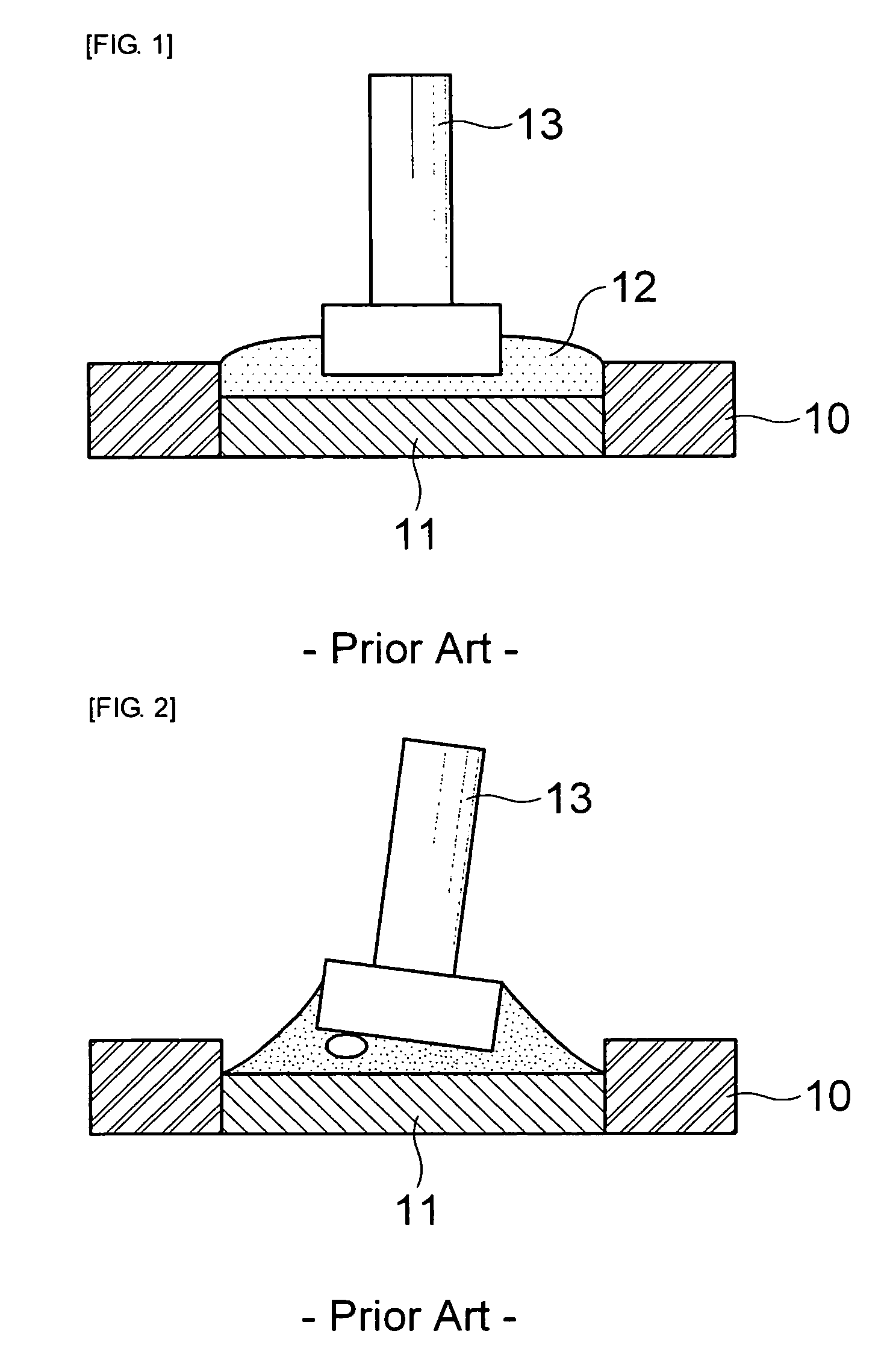
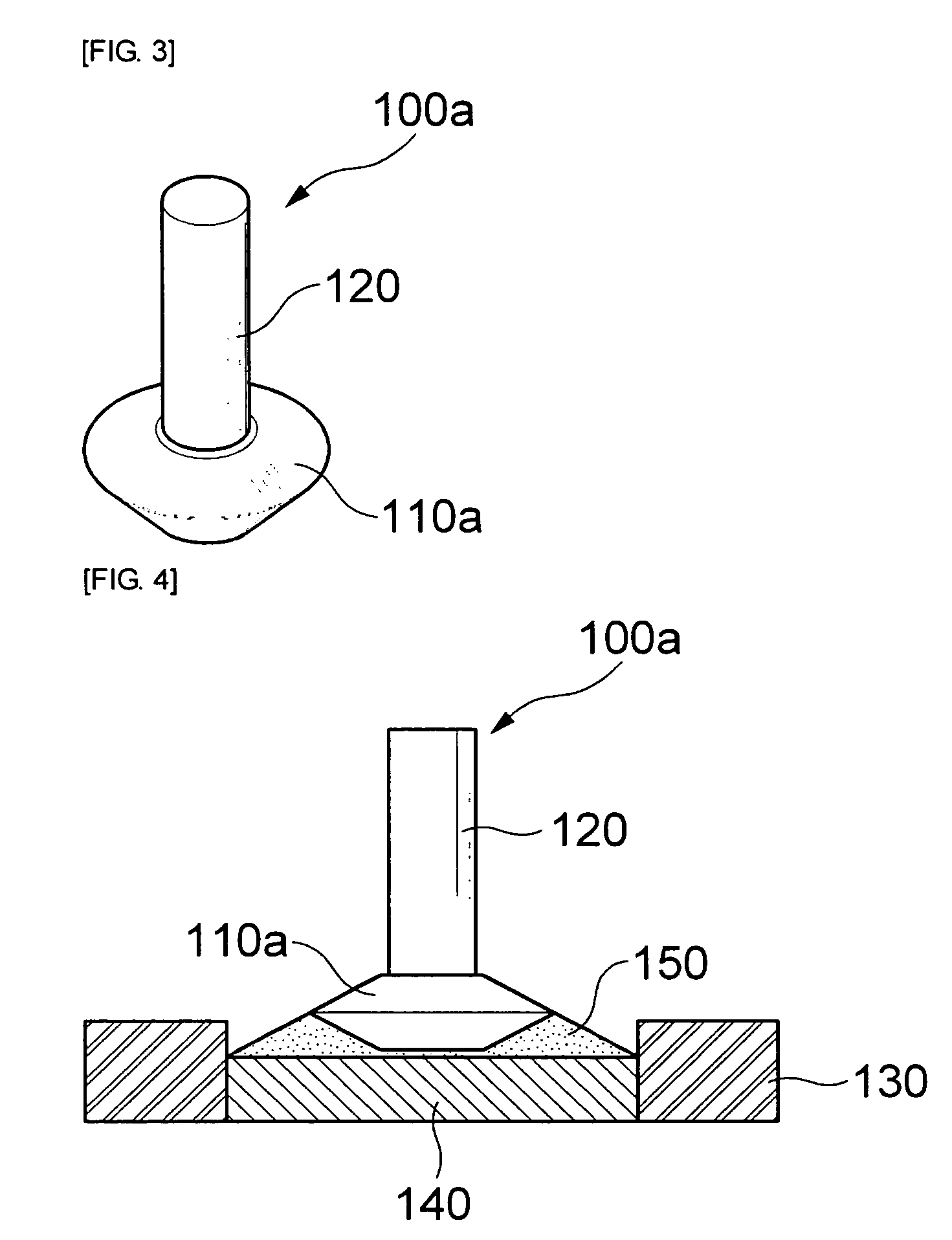
[0034]FIG. 3 is a perspective view of a lead pin for package boards according to the invention. FIG. 4 is a cross-sectional view of the lead pin of FIG. 3, showing a state where the lead pin is bonded to a package board.

[0035]Referring FIGS. 3 and 4, the lead pin 100a includes a connection pin 120 and a head 110a having a larger diameter than the connection pin 120.

[0036]The head 110a has a hexagonal vertical cross-section. The middle portion of the head 110a has a larger diameter than the upper and lower surfaces thereof and the connection pin 120.

[0037]The connection pin 120 is formed so as to project from the center of the upper surface of the head 110a. The height of the connection pin 120 is set to a predetermined value depending on circuit components.

[0038]The lead pin 110a constructed in such a manner is mounted on a package board 130 having an electrode pad portion 140 formed on one surface thereof and a wiring pattern (not shown) formed on the other surface thereof. The ele...

second embodiment

[0046]FIGS. 5A to 5D are perspective views of a lead pin for package boards according to the invention. FIG. 6 is a cross-sectional view of the lead pin of FIG. 5A, showing a state where the lead pin is bonded to a package board.

[0047]Referring to FIGS. 5A to 5D and 6, the lead pin 100b includes a connection pin 120 and a cylindrical head 110b having grooves 113 and 115 formed in the upper and lower portions thereof, respectively.

[0048]The grooves 113 and 115 formed in the upper and lower portions of the head 110b have a semi-circular shape. The grooves 113 formed in the upper portion of the head 110b are symmetrical with respect to the connection pin 120, and the grooves 115 formed in the lower portion of the head 110b are symmetrical with respect to the connection pin 120.

[0049]In this case, two or more grooves 113 and two or more grooves 115 may be formed in the upper and lower portions of the head 110b, respectively. As shown in FIG. 5D, it is preferable that the grooves 113 and...

third embodiment

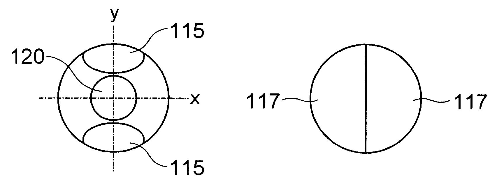
[0055]FIGS. 7A to 7D are perspective views of a lead pin for package boards according to the invention. FIG. 8 is a cross-sectional view of the lead pin of FIG. 7A, showing a state where the lead pin is bonded to a package board.

[0056]Referring to FIGS. 7A to 7D and 8, the lead pin 100c includes a connection pin 120 and a cylindrical head 110c having grooves 115 and 117 formed on the upper and lower surfaces thereof, respectively.

[0057]The grooves 115 and 117 formed on the upper and lower surfaces of the head 110c have a semi-circular shape. The grooves 115 formed on the upper surface of the head 110c are symmetrical with respect to the connection pin 120, and the grooves 117 formed on the lower surface of the head 110c are symmetrical with respect to the connection pin 120.

[0058]In this case, two or more grooves 115 and two or more grooves 117 may be formed on the upper and lower surfaces of the head 110c, respectively. As shown in FIG. 7C, it is preferable that the grooves 115 are...


PUM


Abstract

Provided is a lead pin for package boards including a disk-shaped head of which the diameter increases toward the middle portion thereof and that has a hexagonal vertical cross-sectional shape; and a connection pin that is formed so as to project from the center of the upper surface of the head.

Description

CROSS-REFERENCE TO RELATED APPLICATIONS[0001]This application claims the benefit of Korean Patent Application No. 10-2008-0064245 filed with the Korea Intellectual Property Office on Jul. 3, 2008, the disclosure of which is incorporated herein by reference.BACKGROUND OF THE INVENTION[0002]1. Field of the Invention[0003]The present invention relates to a lead pin for package boards.[0004]2. Description of the Related Art[0005]Recently, a PGA (Pin Grid Array)-type semiconductor package board has been widely used for connecting a package board to a main board, the package board having an IC connected thereto. In the PGA-type semiconductor package board, a lead pin is bonded to a pad portion of the package board through solder.[0006]FIGS. 1 and 2 are process diagrams showing a state where a general package board and a lead pin are bonded to each other.[0007]Referring to FIGS. 1 and 2, solder paste 12 obtained by mixing solder and flux is applied on a pad portion 11 of a package board 10...

Claims


Application Information

Patent Timeline
Patent Type & Authority Patents(United States)
IPC IPC(8): H01R4/18
CPCH01L23/49811H05K3/3426H05K2201/10318Y02P70/613H01L2924/0002H05K2201/10772H01L2924/00Y02P70/50H01L23/48
Inventor OH, HUENG JAECHOI, JIN WON
Owner SAMSUNG ELECTRO MECHANICS CO LTD
Why Eureka
Try Eureka