Circuit and method for VDD-tracking CVDD voltage supply

a technology of cvdd voltage supply and circuit, which is applied in the direction of information storage, static storage, digital storage, etc., can solve the problems of limiting the possible reduction of vdd supply, increasing power consumption and management, and the requirement of voltage supplied to the core array of cells cvdd to limit the possibility of reducing vdd_min

Active Publication Date: 2011-05-31
TAIWAN SEMICON MFG CO LTD
View PDF4 Cites 7 Cited by
  • Summary
  • Abstract
  • Description
  • Claims
  • Application Information

AI Technical Summary

Benefits of technology

[0017]A continuing need thus exists for an improved CVDD and VDD circuitry and methods that provide for robust operation of SRAM arrays, which allow improved VDD_min levels with sufficient static noise margins and that support scalability and design reusability for circuits including SRAM arrays.

Problems solved by technology

Conventional SRAM arrays and embedded SRAM arrays have a fixed voltage requirement for the CVDD supply voltage, and this parameter also necessarily limits the possible reduction in the VDD supply, placing a fixed limit on the important voltage supply parameter of VDD_minimum (VDD_min).
In integrated circuits, power consumption and management of power is increasingly a critical issue.
However, in conventional SRAM arrays such as those created using SRAM compilers, the voltage supplied to the core array of cells CVDD has requirements that limit the possible reduction in VDD_min.
The difference between the voltage supplied to the core array, and that of the VDD supply to the logic circuitry surrounding and in communication with the SRAM cells can cause erroneous operation of the SRAM if it becomes too large.
This means VDD_min cannot be reduced too far below CVDD.
This means that VDD_min cannot be reduced when CVDD is fixed.
However, in this example, the lowered VDD value on the bit lines has a negative impact on operation of the SRAM cell.
The prior art approaches fail to take advantage of the benefits of scaling during design “shrinks” as is commonly done to improve circuit performance when using more advanced semiconductor processes.

Method used


Image

  • Circuit and method for VDD-tracking CVDD voltage supply
  • Circuit and method for VDD-tracking CVDD voltage supply
  • Circuit and method for VDD-tracking CVDD voltage supply

Examples


Embodiment Construction

[0036]The making and using of the presently preferred embodiments are discussed in detail below. It should be appreciated, however, that the present invention provides many applicable inventive concepts that can be embodied in a wide variety of specific contexts. The specific embodiments discussed are merely illustrative of specific ways to make and use the invention, and do not limit the scope of the invention.

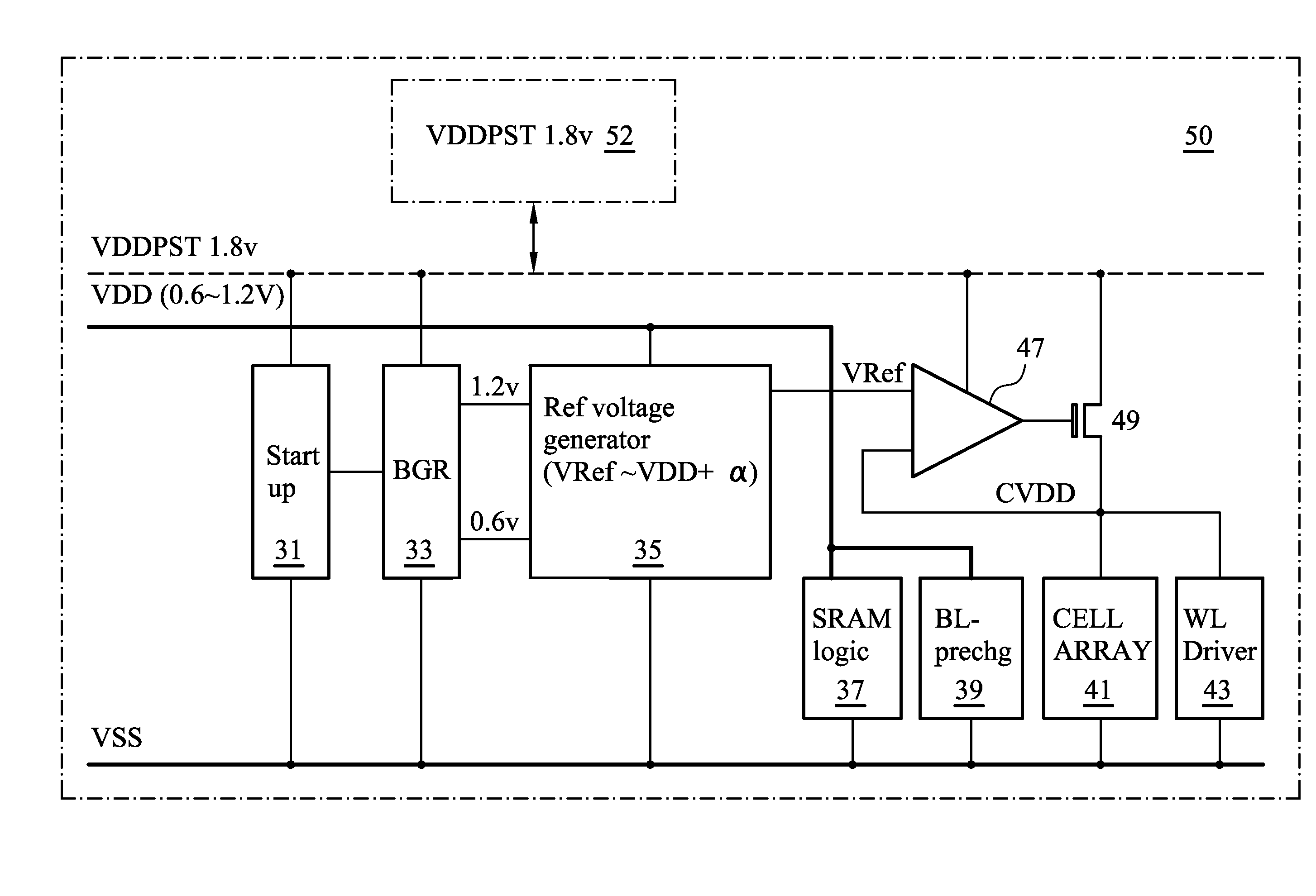
[0037]FIG. 5 depicts in a circuit diagram an exemplary embodiment of a dual rail VDD tracking CVDD circuit for an SRAM array or SRAM circuit 50. In FIG. 5, an external supply voltage VDDPST of 1.8 Volts, for example, is shown. Supply voltage VDD which is used by various logic circuitry, such as SRAM logic 37, is provided as low as possible. In this example, a range from about 0.6 Volts to 1.2 Volts is indicated. Future process nodes may operate at lower VDD voltages. A startup circuit 31 and a band gap reference circuit BGR 33 are shown coupled together to supply two voltages...


PUM


Abstract

Circuit and methods for providing the CVDD supply to the cells in an SRAM array while maintaining a desired VDD voltage. A circuit is described for tracking the VDD supply voltage and providing a CVDD supply for the SRAM cells that maintains an offset above VDD until a maximum voltage for the CVDD voltage is reached. The CVDD voltage supplies the word line drivers and the cells in an SRAM array, while the bit line precharge and the remaining circuitry is operated on the VDD supply. By maintaining a maximum offset between the voltage CVDD and the supply voltage VDD, the SRAM will have the required static noise margins for reliable operation, while a lowered VDD_min voltage may also be obtained. A method for supplying a CVDD voltage to an SRAM cell array is disclosed where the CVDD voltage tracks a VDD supply voltage plus a predetermined offset voltage.

Description

[0001]This application claims the benefit of U.S. Provisional Application No. 61 / 074,917 filed on Jun. 23, 2008, entitled “VDD-Tracking CVDD Dual Rail SRAM Design,” which application is hereby incorporated herein by reference.TECHNICAL FIELD[0002]The present invention relates to circuits and methods for providing improved memory core positive voltage supply (CVDD) regulation to SRAM arrays. SRAM arrays are often embedded in present day integrated circuits with added logic circuitry, macros such as DSPs and processors, analog front end and other circuits. Often, silicon compilers or similar automated design tools are used to specify the SRAM arrays. As semiconductor process technology advances, increasingly circuit compilation tools are used and ideally the SRAM designs created by these tools are reusable and scalable to different processes to enhance performance without redesign. Conventional SRAM arrays and embedded SRAM arrays have a fixed voltage requirement for the CVDD supply v...

Claims


Application Information

Patent Timeline
Patent Type & Authority Patents(United States)
IPC IPC(8): G11C5/14
CPCG11C11/413G11C5/147
Inventor CHEN, YEN-HUEICHAN, WEI MINCHOU, SHAO-YU
Owner TAIWAN SEMICON MFG CO LTD
Why Eureka
Try Eureka