Technique for photonic analog-to-digital signal conversion

a technology of analog-to-digital signal and photonics, applied in analogue/digital conversion, transmission systems, instruments, etc., can solve the problems of affecting the accuracy of tracking by a tha, increasing with sampling rate, corrupting the performance of adc b>100/b>, etc., and achieving the effect of reducing sampling jitter

Inactive Publication Date: 2011-06-07
RPX CORP +1
View PDF6 Cites 18 Cited by
  • Summary
  • Abstract
  • Description
  • Claims
  • Application Information

AI Technical Summary

Benefits of technology

[0006]The invention overcomes the above-identified shortcomings by using M>1 sampling devices (e.g., THAs) in a photonic ADC to sample an analog signal input in a time-interleaved fashion. Advantageously, the sampling frequency at which each of the sampling devices operates is a fraction (e.g., 1 / M) of fs used in ADC 100, thereby reducing the sampling jitter. In accordance with the invention, multiple optical clock signals having the same frequency (e.g., fs / M) but various clock phases are used in a photonic ADC. Each of the optical clock signals is associated with a respective one of the M sampling devices. The M sampling devices successively sample the analog signal input to provide samples thereof. The sampling operation by each sampling device is time-controlled by the optical clock signal associated with the sampling device. The resulting samples from the sampling devices being processed to provide quantized samples. The inventive ADC produces a digital signal output representing values of the quantized samples.

Problems solved by technology

One such shortcoming stems from the fact that sampling jitter, which adversely affects the precision of tracking by a THA of an analog signal input, increases with the sampling rate of the THA.
Thus, as the sampling rate of THA 105 (fs) is required to increase over time to meet the demand for higher digital quality, more and more sampling jitter is introduced to THA 105, thereby corrupting the performance of ADC 100, which is undesirable.
As a result, the propagation of clock signals through some significantly different signal path lengths causes clock jitter which further corrupts the performance of ADC 100.

Method used


Image

  • Technique for photonic analog-to-digital signal conversion
  • Technique for photonic analog-to-digital signal conversion
  • Technique for photonic analog-to-digital signal conversion

Examples


Embodiment Construction

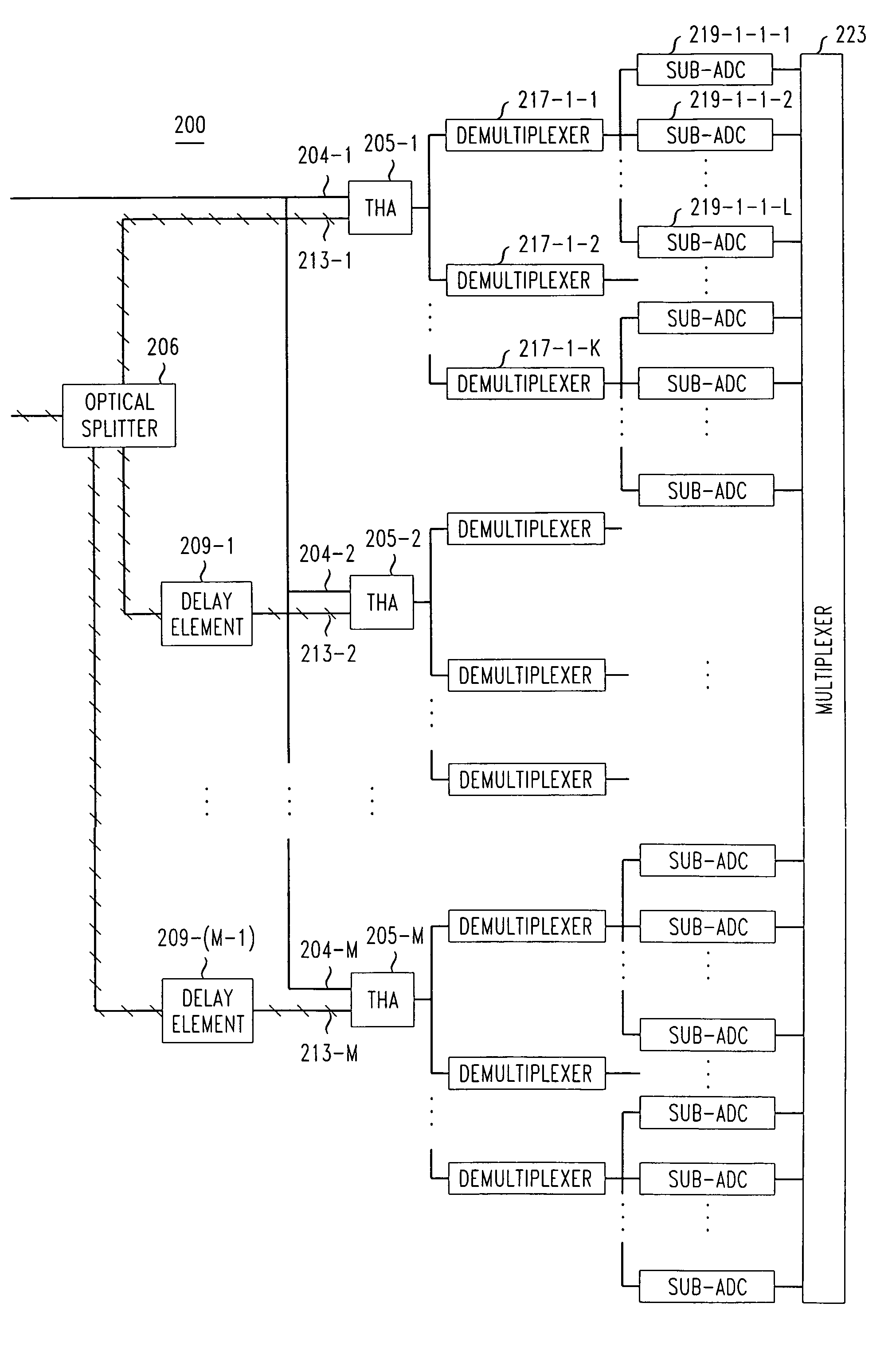
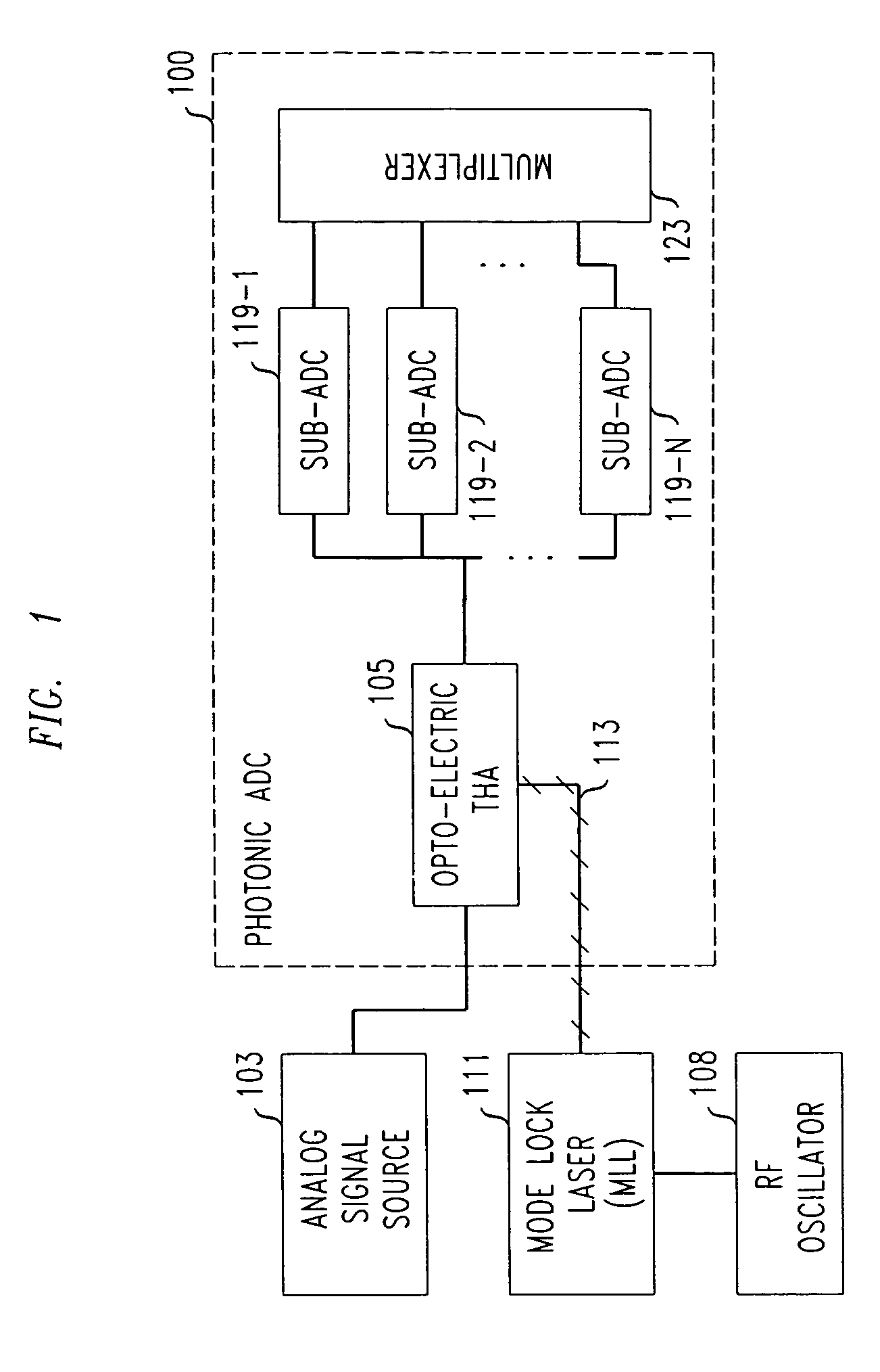
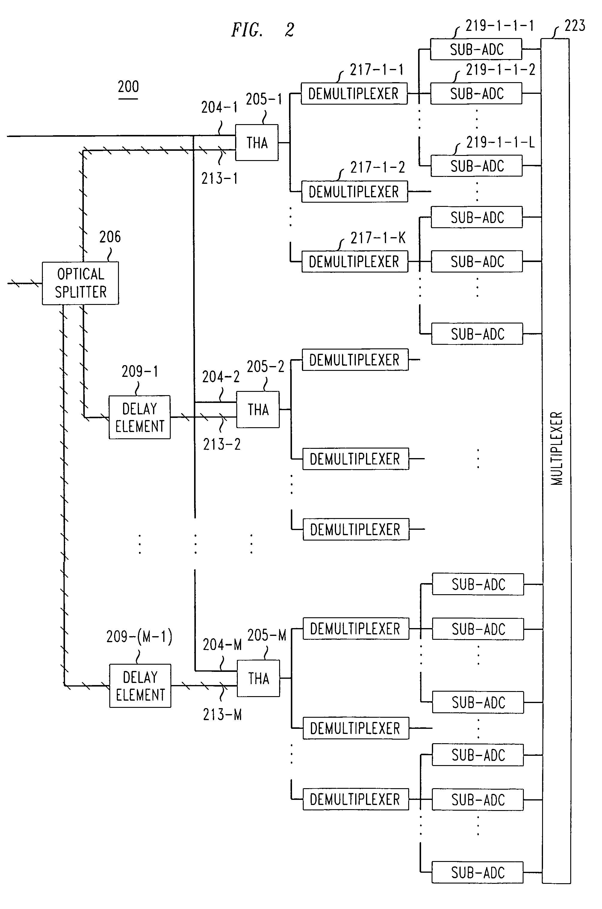
[0014]FIG. 2 is a block diagram which illustrates photonic ADC 200 embodying the principles of the invention. Unlike ADC 100, photonic ADC 200 employs multiple opto-electric track and hold amplifiers (THAs) to perform time-interleaved photonic sampling in accordance with the invention. To that end, an analog signal (e.g., from analog signal source 103) to be digitized by ADC 200 is fed via electric waveguides 204-1, 204-2, . . . , 204-M to M different opto-electric THAs, denoted 205-1, 205-2, . . . , 205-M, respectively, where M>1. Because of use of the M THAs in accordance with the invention, the sampling rate required of each THA here is fs / M Hz, as opposed to the fs Hz sampling rate of THA 105 in ADC 100. As a result, ADC 200 here is subject to significantly less sampling jitter, compared with ADC 100.

[0015]An optical clock signal of a frequency fs / M Hz from an external source (e.g., from MLL driven by an Rf oscillator of the corresponding frequency) is provided to ADC 200 for ac...


PUM


Abstract

In an inventive photonic analog-to-digital signal converter (ADC), multiple opto-electric sampling devices are employed to successively sample an analog signal input. Optical clock signals having the same frequency but different clock phases are used, which are associated with the opto-electric sampling devices, respectively. Each sampling device takes samples of the analog signal input in response to the optical clock signal associated therewith. The resulting samples are processed to produce quantized samples. The inventive ADC outputs a digital signal representing the quantized samples.

Description

FIELD OF THE INVENTION[0001]The invention relates to a technique for signal processing and, in particular, to a technique for analog-to-digital signal conversion using optical clocking.BACKGROUND OF THE INVENTION[0002]This section introduces aspects that may help facilitate a better understanding of the invention. Accordingly, the statements of this section are to be read in this light and are not to be understood as admissions about what is prior art or what is not prior art.[0003]Digital media (e.g., digital audio, image and video) have become an integral part of our daily life. Increasingly high speed digital signal processors and computers, and sophisticated coding techniques (e.g., MP3, JPEG, MPEG2, etc.) lend great support to the proliferation of use of digital media. Analog-to-digital signal converters (ADCs) are essential for transforming the analog media we perceive to the digital media to take advantage of the advanced digital technology. As people demand higher and higher...

Claims


Application Information

Patent Timeline
Patent Type & Authority Patents(United States)
IPC IPC(8): H03M1/12
CPCG02F7/00H03M1/1215
Inventor LEE, JAESIKCHEN, YOUNG-KAI
Owner RPX CORP
Why Eureka
Try Eureka