
Eureka
For R&D, Eureka makes reading and utilizing patents & technical documents easy.
Eureka AIR
Designed for self-driven R&D workflows. Generate viable solutions, solve complex R&D challenges, empower your innovation with AI.

Eureka Materials
Designed for material experts only. Revolutionize your material R&D, from search, analyze, to developing new materials.

TechResearch
Generate reliable direction feasibility study reports for your R&D in just a few steps.

TechSeek
Discover and master advanced knowledge NOW. Basics, ideas, possibilities, all at once.

TechMind
As an expert in R&D Theories, TechMind can generates customized viable solutions instantly.

TechRisk
Analyze your overall solution with one click, know your potential R&D risks in advance.

TechMonitor
Get weekly tech updates, stay abreast of the latest tech innovations and key insights.
Organic light emitting diode display device having organic layers of varying thickness
a technology of light-emitting diodes and display devices, which is applied in the direction of discharge tubes luminescnet screens, test/measurement of semiconductor/solid-state devices, natural mineral-layered products, etc., can solve the problems of difficult to improve the luminous efficiency and luminance of a displayed, low-resolution small-sized display devices, and degraded color coordinates. , to achieve the effect of enhancing color coordinates and improving the luminous efficiency and luminance of the displayed whi
- Summary
- Abstract
- Description
- Claims
- Application Information
AI Technical Summary
Benefits of technology
Problems solved by technology
Method used
Image

Examples
embodiment 1
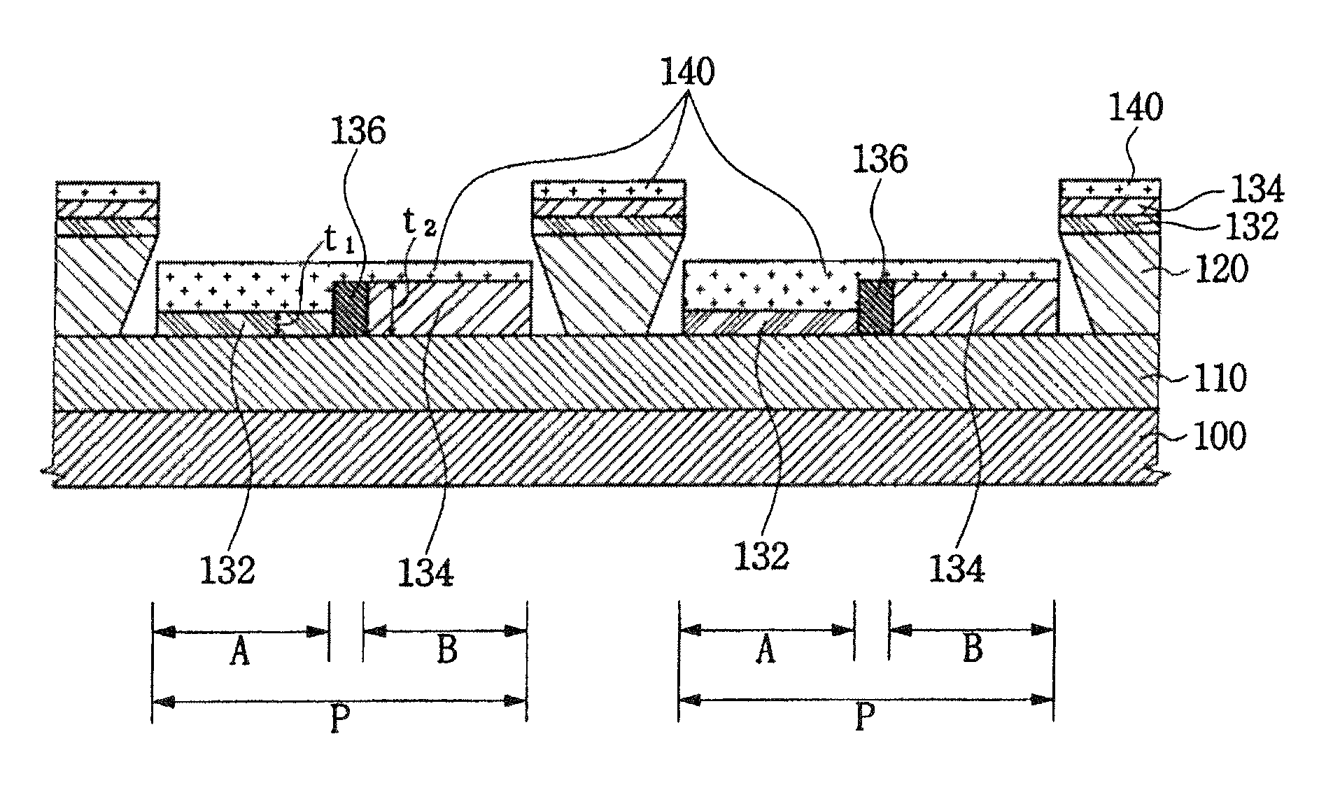
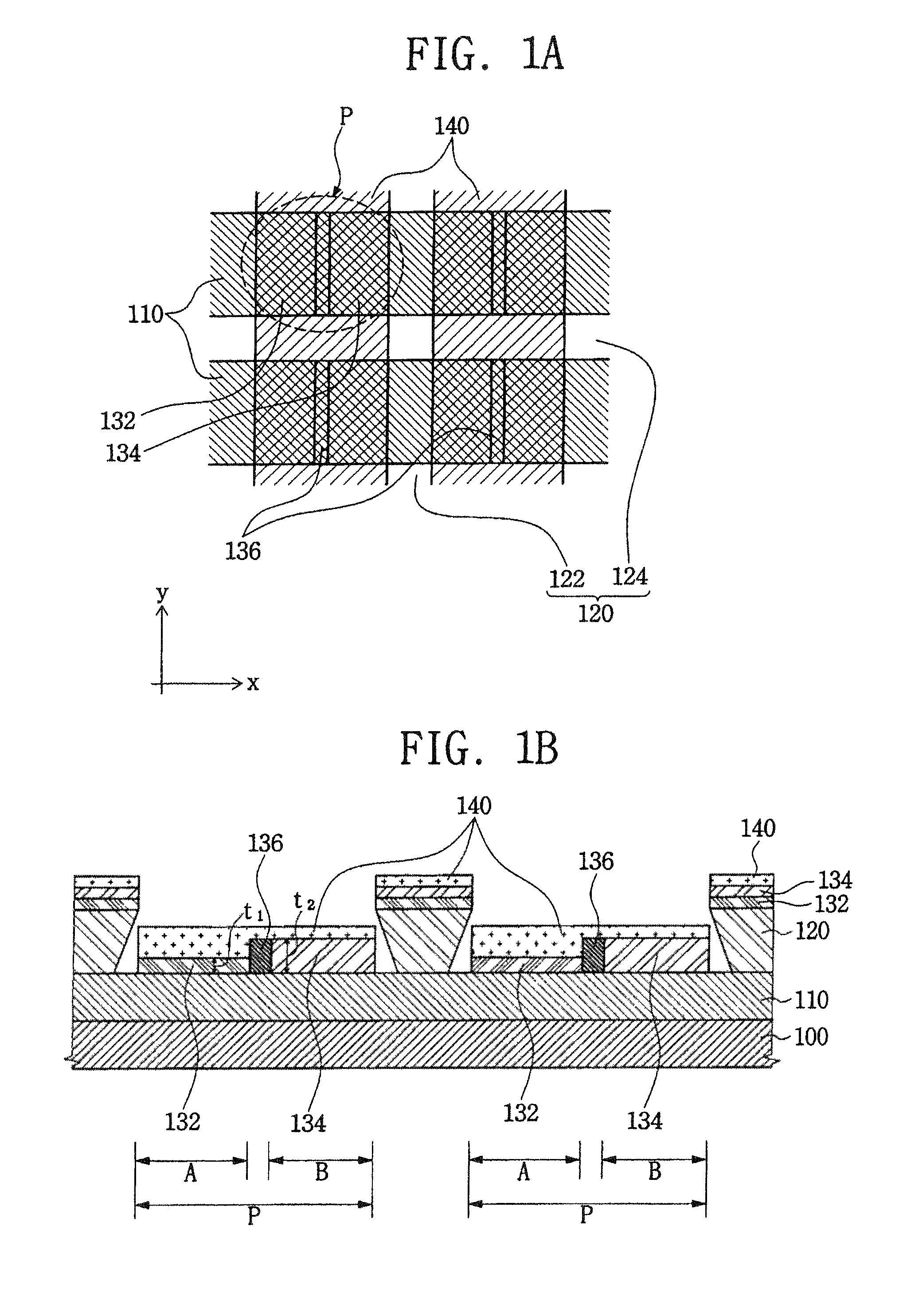
FIG. 1A is a plan schematic view of an organic light emitting diode (OLED) display device according to an exemplary embodiment of the present invention, and FIG. 1B is a cross-sectional schematic view taken along line I-I′ of FIG. 1A.
Referring to FIGS. 1A and 1B, the OLED display device includes a substrate 100 and a lower (or first) electrode 110 disposed on the substrate 100 and disposed (or extending) in a first direction “x”. An upper (or second) electrode 140 is disposed (or extending) in a second direction “y” crossing (or orthogonal to) the first direction “x”. A separator 120 is interposed between the lower electrode 110 disposed in the first direction “x” and the upper electrode 140 disposed in the second direction “y” and separates a plurality of pixel regions P from one another. A first organic layer 132 is interposed between the lower and upper electrodes 110 and 140 and has a first thickness t1. A second organic layer 134 is interposed between the lower and upper electr...
embodiment 2
FIG. 3 is cross-sectional schematic view according to another exemplary embodiment of the present invention.
Referring to FIG. 3, the OLED display device includes a substrate 300 and a thin film transistor (TFT) disposed on the substrate 300. The TFT includes a semiconductor layer 320, a gate insulating layer 330, a source electrode 352, a drain electrode 354, and a gate electrode 336. A first insulating layer 360 is disposed on the TFT. A lower (or first) electrode 370 is disposed on the first insulating layer 360. A first organic layer 380a is disposed on a first region C of the lower electrode 370 and has a first thickness t3. A second organic layer 380b is disposed on a second region D of the lower electrode 370 and has a second thickness t4 different from the first thickness t3. An upper (or second) electrode 390 is disposed on the resultant structure having the second organic layer 380b. Although the second thickness t4 of the second organic layer 480a is illustrated as being g...
embodiment 3
FIG. 5 is a cross-sectional schematic view of an OLED display device according to another exemplary embodiment of the present invention.
Referring to FIG. 5, the OLED display device includes a substrate 500. A lower (or first) electrode 570 is disposed on the substrate 500. A thin film transistor (TFT) may be also disposed on the substrate 500 and / or between the lower electrode 570 and the substrate 500. A first organic layer 580a is disposed on a first region of the lower electrode 570 and has a first thickness. A second organic layer 580b is disposed on a second region of the lower electrode 570 and has a second thickness different from the first thickness. An upper (or second) electrode 590 is disposed on the resultant structure having the second organic layer 580b. Here, as shown, the first organic layer 580a and the second organic layer 580b are laterally separated from each other by an insulating layer 585, and a side of the first organic layer 580a facing a side of the lower e...
PUM
| Property | Measurement | Unit |
|---|---|---|
| thickness | aaaaa | aaaaa |
| refractive indices | aaaaa | aaaaa |
| refractive index | aaaaa | aaaaa |
Abstract
Description
Claims
Application Information
 - R&D Engineer
- R&D Manager
- IP Professional
- Industry Leading Data Capabilities
- Powerful AI technology
- Patent DNA Extraction
Browse by: Latest US Patents, China's latest patents, Technical Efficacy Thesaurus, Application Domain, Technology Topic, Popular Technical Reports.
© 2024 PatSnap. All rights reserved.Legal|Privacy policy|Modern Slavery Act Transparency Statement|Sitemap|About US| Contact US: help@patsnap.com