
Eureka
For R&D, Eureka makes reading and utilizing patents & technical documents easy.
Eureka AIR
Designed for self-driven R&D workflows. Generate viable solutions, solve complex R&D challenges, empower your innovation with AI.

Eureka Materials
Designed for material experts only. Revolutionize your material R&D, from search, analyze, to developing new materials.

TechResearch
Generate reliable direction feasibility study reports for your R&D in just a few steps.

TechSeek
Discover and master advanced knowledge NOW. Basics, ideas, possibilities, all at once.

TechMind
As an expert in R&D Theories, TechMind can generates customized viable solutions instantly.

TechRisk
Analyze your overall solution with one click, know your potential R&D risks in advance.

TechMonitor
Get weekly tech updates, stay abreast of the latest tech innovations and key insights.
Organic electroluminescent device and organic electroluminescent display device
a technology of electroluminescent display device and electroluminescent device, which is applied in the direction of discharge tube luminescnet screen, discharge tube/lamp details, electric discharge lamps, etc., can solve the problems of limited application, inadequate above-mentioned measures, and insufficient common organic el devices, so as to improve the luminous efficiency and luminance and extend the lifetime of the organic el devices.
- Summary
- Abstract
- Description
- Claims
- Application Information
AI Technical Summary
Benefits of technology
Problems solved by technology
Method used
Image

Examples
embodiment 1
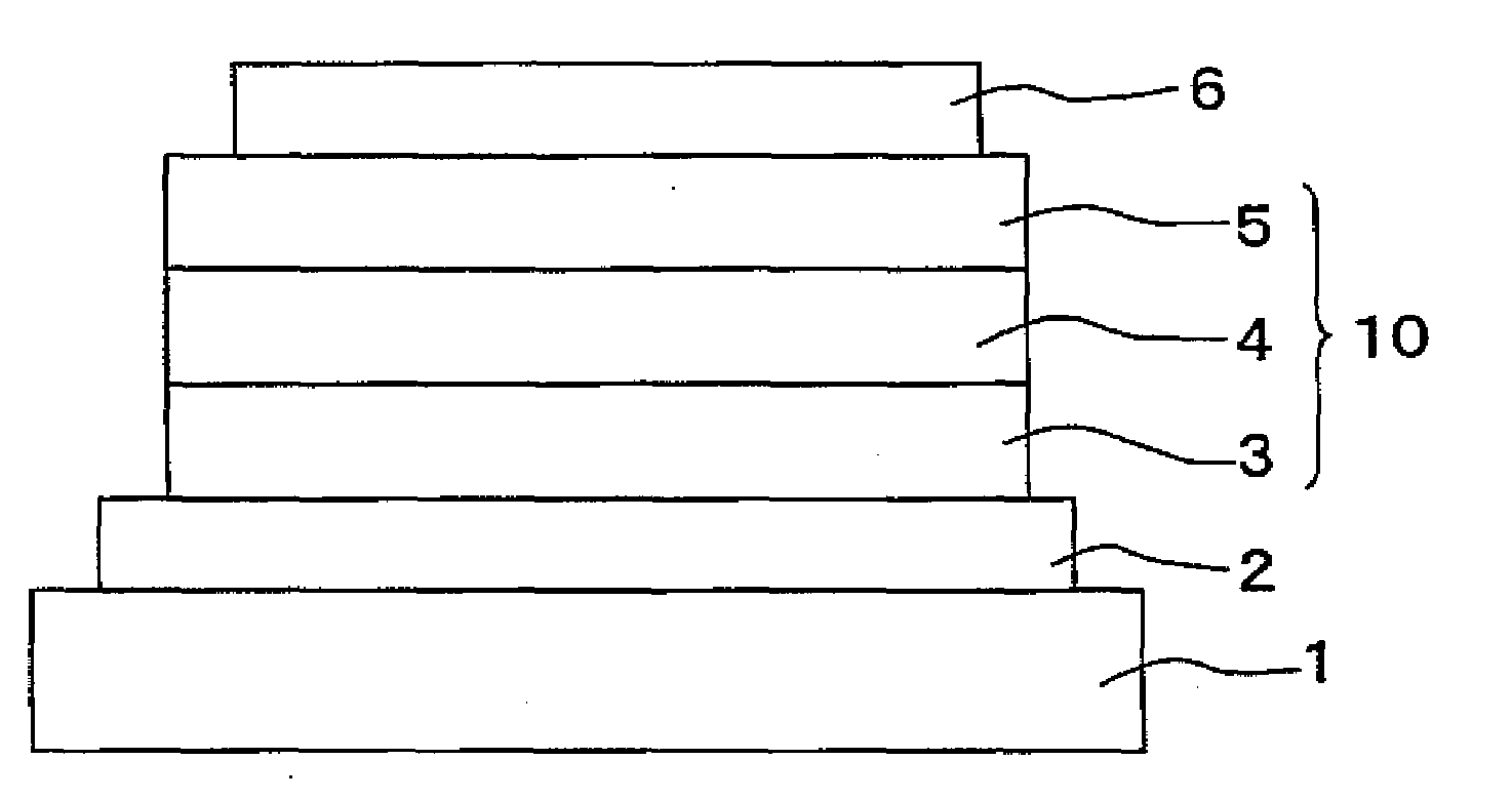
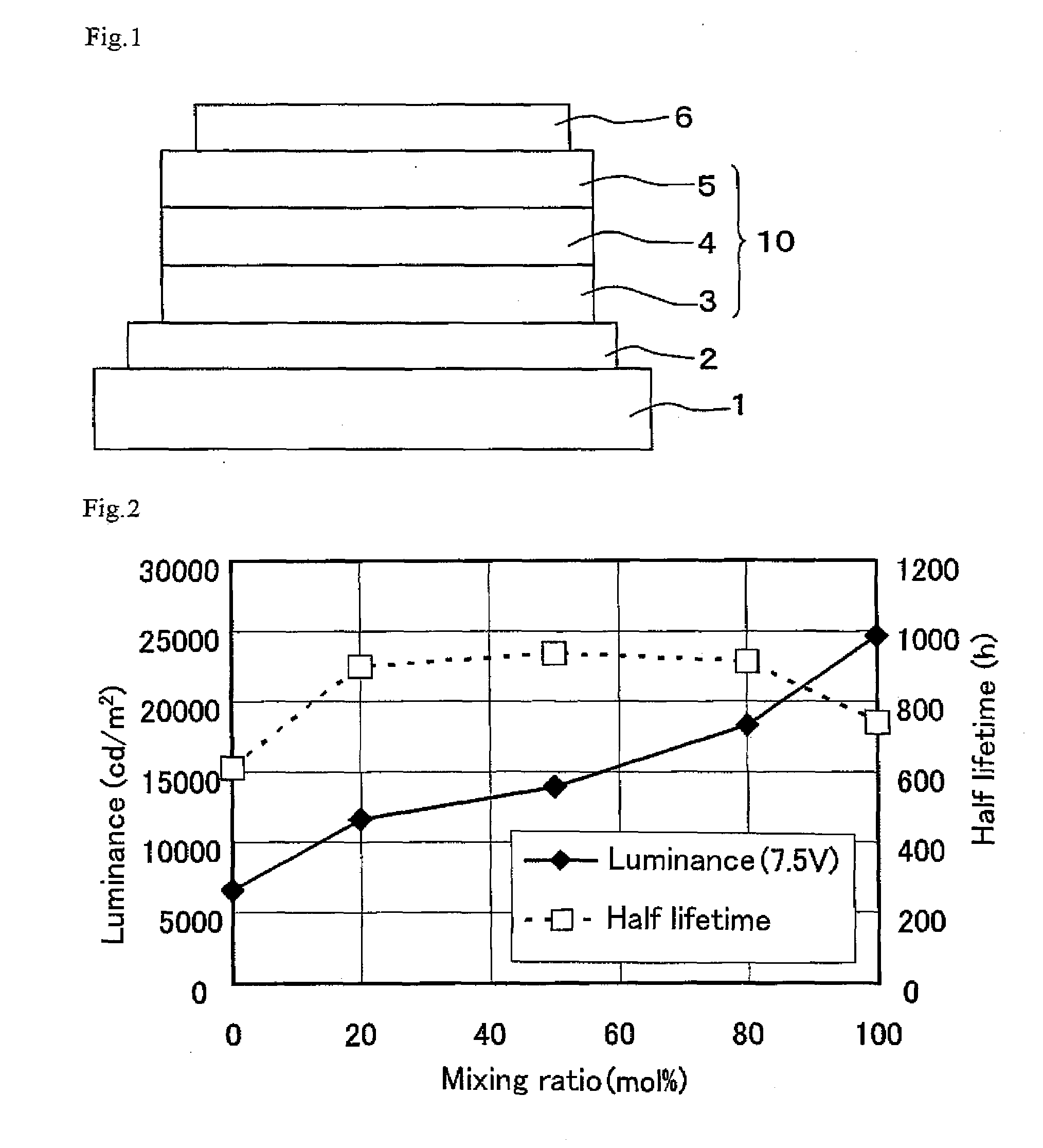
[0027]FIG. 1 is a schematic sectional view of the organic EL device of Embodiment 1.
[0028]The organic EL device of the present embodiment has a layered structure in which an anode 2, an organic layer 10 which is a layered body including a hole injection layer 3, a hole transport layer 4 and a light-emitting layer 5, and a cathode 6 are located on a substrate 1 in turn. Thus, in the organic layer 10, since the light-emitting layer 5 is separated from the hole injection layer 3, injection efficiency of the hole into the light-emitting layer 5 is improved. Further, since the hole transport layer 4 is located between the light-emitting layer 5 and hole injection layer 3, injection efficiency of the hole into the light-emitting layer 5 is improved. Consequently, in the organic EL device of this Embodiment, the luminance and the luminous efficiency can be increased compared to the organic EL device in which the hole injection layer 3 and the hole transport layer 4 are not arrange. Further...
example 1
[0040]A method of producing an organic EL device of Example 1 will be described.
[0041]First, an anode 2 was formed on a substrate 1 having a insulating surface. In this example, a substrate with electrodes, in which an ITO electrode had been previously formed on the surface of a glass substrate of 30×30 mm square as an anode 2, was prepared and cleaned. As for cleaning of the substrate with electrodes, ultrasonic cleaning was performed for 10 minutes and then UV-ozone cleaning was performed for 30 minutes using acetone and isopropyl alcohol.
[0042]Next, a hole injection layer 3 of 60 nm in thickness was formed on the surface of the anode 2. First, a coating solution for forming a hole injection layer was prepared by dispersing PEDOT / PSS in pure water. This coating solution for forming a hole injection layer was applied onto the surface of the anode 2 using a spin coater. Thereafter, a solvent in the coating solution for forming a hole injection layer was removed by heating / drying (20...
example 2
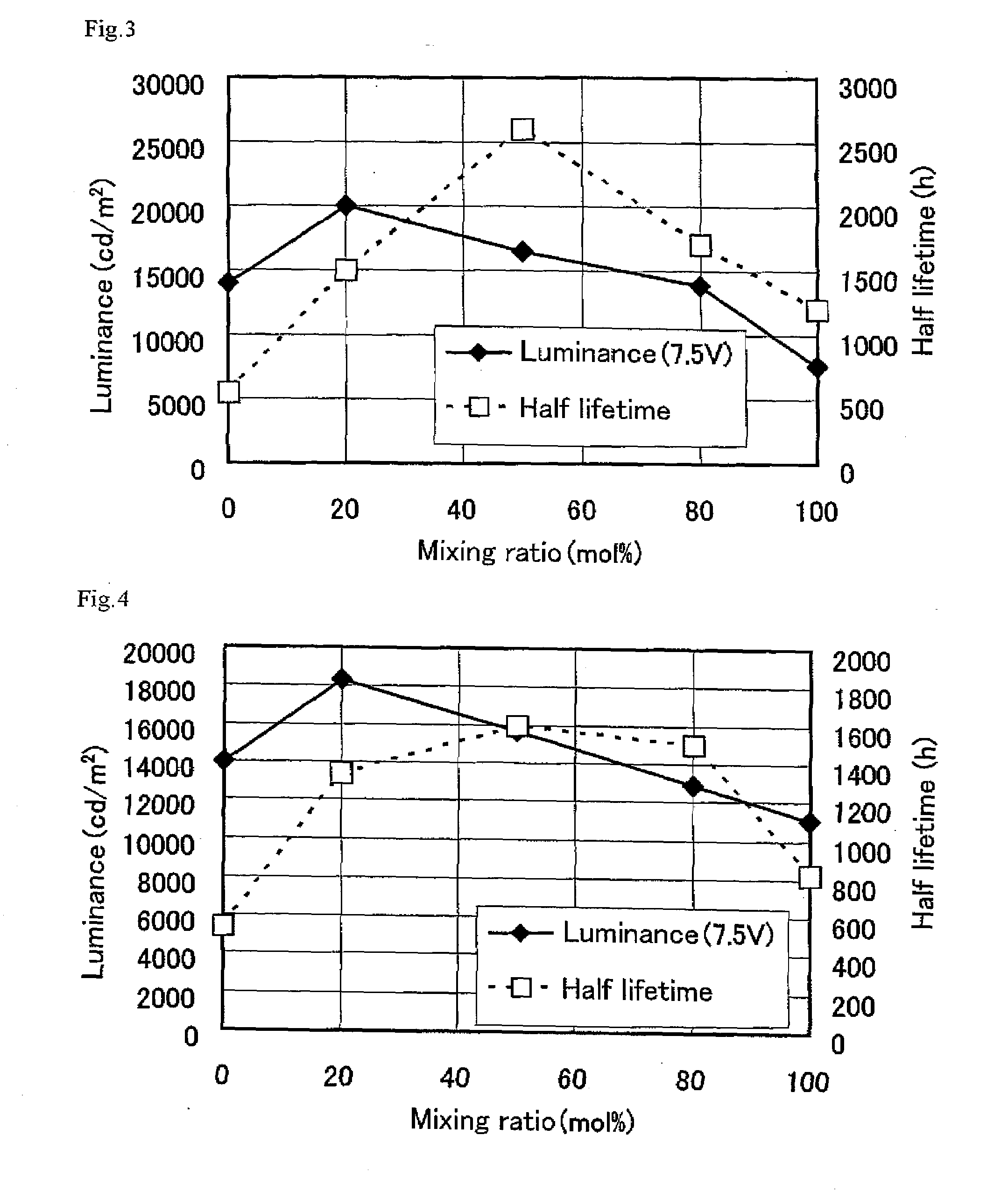
[0047]Since the constitution of an organic EL device of Example 2 is similar to that of Example 1 and the light-emitting materials contained in the light-emitting layers 5 are just different from each other, the descriptions of overlapping contents between Example 1 and Example 2 will be omitted.
[0048]The light-emitting layer 5 of this example was prepared using a coating solution for forming a light-emitting layer prepared by dissolving an hole transport blue light-emitting polymer material (fluorescent material; a poly(triphenylamine) derivative) containing a chromophore having a luminance peak at a wavelength of 464 nm and an electron transport blue light-emitting polymer material (fluorescent material; poly(fluorene-anthracene)) containing a chromophore having a luminance peak at a wavelength of 466 nm in xylene. As described above, all of the light-emitting materials in this example are a fluorescent material.
PUM
 Abstract
Description
Claims
Application Information
 - R&D Engineer
- R&D Manager
- IP Professional
- Industry Leading Data Capabilities
- Powerful AI technology
- Patent DNA Extraction
Browse by: Latest US Patents, China's latest patents, Technical Efficacy Thesaurus, Application Domain, Technology Topic, Popular Technical Reports.
© 2024 PatSnap. All rights reserved.Legal|Privacy policy|Modern Slavery Act Transparency Statement|Sitemap|About US| Contact US: help@patsnap.com