Providing an organic electroluminescent device having stacked electroluminescent units

a technology of electroluminescent units and organic materials, which is applied in the direction of discharge tube luminescnet screens, natural mineral layered products, transportation and packaging, etc., can solve the problems of unavoidable trade-off between luminance and operational life, the total current requirements of the device are not reduced, and the luminance efficiency in terms of candela per ampere (cd/a) is actually not improved

Inactive Publication Date: 2005-03-29
EASTMAN KODAK CO
View PDF51 Cites 347 Cited by
  • Summary
  • Abstract
  • Description
  • Claims
  • Application Information

AI Technical Summary

Benefits of technology

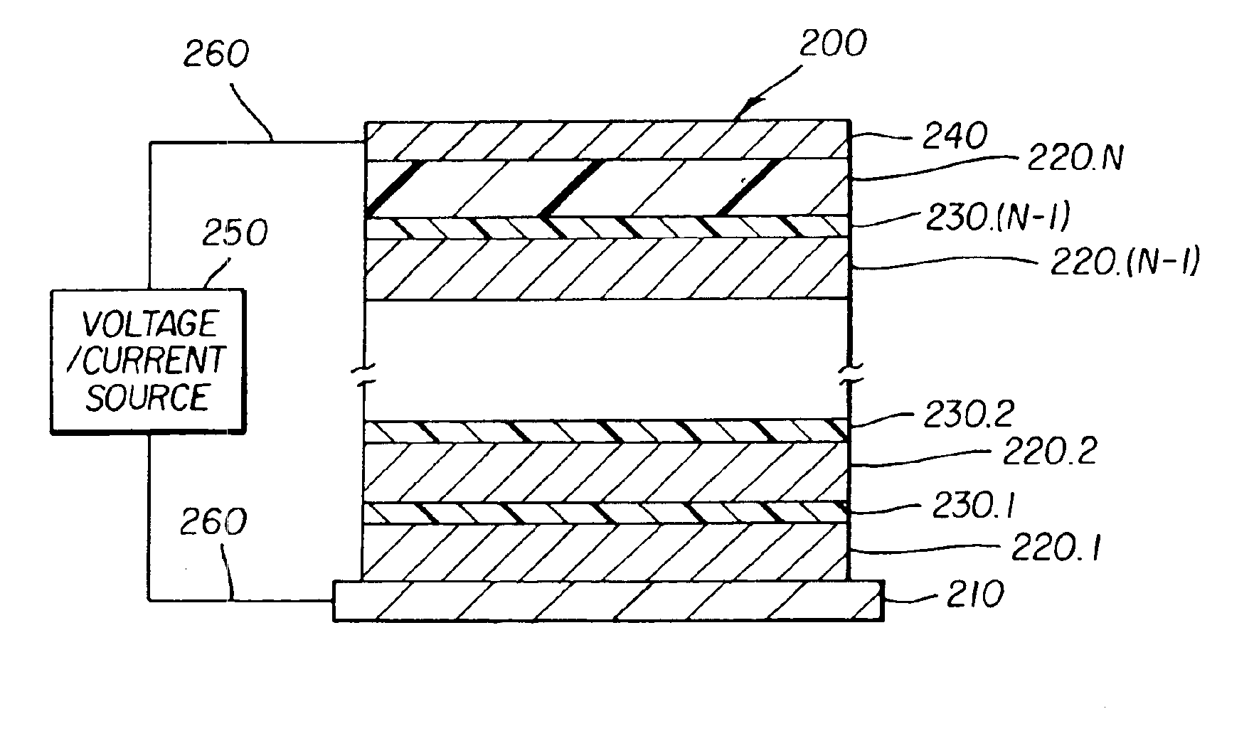
An advantage of the present invention is that it enables a stacked OLED to function without requiring intra-electrodes, thereby lowering optical losses.
is that it enables a stacked OLED to function without requiring intra-electrodes, thereby lowering optical losses.
Another advantage of the present invention is that the stacked OLED device provides significantly improved luminance efficiency measured in cd / A compared to the conventional non-stacked OLED device.
Another advantage of the present invention is that the stacked OLED has an increased brightness if operated under the same current as that of the conventional OLED.
Another advantage is that the stacked OLED has an increased lifetime if operated under the same brightness as that of the conventional OLED.
Another advantage of the present invention is that the stacked OLED has a decreased driving voltage and an increased optical output compared to the prior arts of stacked OLEDs.

Problems solved by technology

Thus, there is unavoidable tradeoff between luminance and operational lifetime.
However, the total current requirements for the device are not reduced, and the luminance efficiency in terms of candela per ampere (cd / A) is actually not improved.
While this enables higher luminance, the overall construction of the OLED device is complex, requiring transparent electrodes as well as separate power source for each of the stacked OLED units.
The use of metallic or inorganic intra-electrodes in the stacked OLED of Forrest et al. or Burrows et al. poses several problems.
First, it requires complex wiring in order to address each OLED unit in the stack.
Second, the electrode layers between the OLED units in the stack absorb light, and if made too thick, create optical losses that decrease overall light output efficiency.
So-called transparent electrodes are known but still absorb significant levels of light and are difficult to fabricate over organic structures.
In fact, Burrows et al. show by mathematical modeling the serious decrease in luminance efficiency caused by the expected optical losses due to the intra-electrode layers.
Third, if the electrode is made too thin to improve optical properties, the sheet resistance is too high rendering high driving voltage for each individual OLED element and uneven luminance inside the device area.
While this alleviates the complex wiring problems of U.S. Pat. No. 5,703,436 and U.S. Pat. No. 6,274,980, the device disclosed by Jones et al. suffers the same optical problems as noted above.

Method used


Image

  • Providing an organic electroluminescent device having stacked electroluminescent units
  • Providing an organic electroluminescent device having stacked electroluminescent units
  • Providing an organic electroluminescent device having stacked electroluminescent units

Examples


example 1

Conventional OLED—Comparative

The preparation of a conventional non-stacked OLED is as follows: A 1 mm thick glass substrate coated with a transparent ITO conductive layer was cleaned and dried using a commercial glass scrubber tool. The thickness of ITO is about 42 nm and the sheet resistance of the ITO is about 68 Ω / square. The ITO surface was subsequently treated with oxidative plasma to condition the surface as an anode. A layer of CFx, 1 nm thick, was deposited on the clean ITO surface as the HIL by decomposing CHF3 gas in RF plasma treatment chamber. The substrate was then transferred into a vacuum deposition chamber for deposition of all other layers on top of the substrate. The following layers were deposited in the following sequence by sublimation from a heated boat under a vacuum of approximately 10−6 Torr:(1) a HTL, 75 nm thick, consisting of NPB;(2) an ETL (also serving as the emissive layer), 60 nm thick, consisting of Alq;(3) a cathode, approximately 210 nm thick, cons...

example 2

Comparative

A stacked OLED was fabricated with the following sequential layers:(1) a HTL, 50 nm thick, consisting of NPB;(2) an ETL (also serving as the emissive layer), 50 nm thick, consisting of Alq;(3) a thin metal electrode, 1 nm thick, consisting of Mg:Ag;(4) another thin metal electrode, 1.5 nm thick, consisting of Ag;(5) a HTL, 50 nm thick, consisting of NPB;(6) an ETL (also serving as the emissive layer), 50 nm thick, consisting of Alq;(7) a cathode, approximately 210 nm thick, consisting of Mg:Ag.

The processing steps other than the aforementioned layer deposition were the same as Example 1. The stacked device structure is denoted as ITO / CFx / NPB(50) / Alq(50) / Mg:Ag / Ag / NPB(50) / Alq(50) / Mg:Ag.

This stacked OLED requires a driving voltage of 21.2 V to pass 20 mA / cm2. Its EL efficiency is 0.1 cd / A. Its luminance efficiency-current characteristic, indicated as Example 2, is shown in FIG. 6.

example 3

Comparative

A stacked OLED was fabricated with the following sequential layers:(1) a HTL, 75 nm thick, consisting of NPB;(2) an ETL (also serving as the emissive layer), 60 nm thick, consisting of Alq;(3) a metal electrode, 10 nm thick, consisting of Mg;(4) a HTL, 75 nm thick, consisting of NPB;(5) an ETL (also serving as the emissive layer), 60 mm thick, consisting of Alq;(6) a cathode, approximately 210 nm thick, consisting of Mg:Ag.

The processing steps other than the aforementioned layer deposition were the same as Example 1. The stacked device structure is denoted as ITO / CFx / NPB(75) / Alq(60) / Mg / NPB(75) / Alq(60) / Mg:Ag.

The stacked OLED has a driving voltage of 11.2 V, a current density of 20 mA / cm2, and an EL efficiency of 1.3 cd / A. Its luminance efficiency-current characteristic, indicated as Example 3, is shown in FIG. 6.


PUM

PropertyMeasurementUnit
thicknessaaaaaaaaaa
thicknessaaaaaaaaaa
work functionaaaaaaaaaa

Abstract

A stacked organic electroluminescent device and a method of making such device is disclosed. The device comprises an anode, a cathode, at least two organic electroluminescent units disposed between the anode and the cathode, and a doped organic connector disposed between each adjacent organic electroluminescent unit wherein the organic electroluminescent unit comprises at least one organic hole-transporting layer and one organic electron-transporting layer. The doped organic connector comprises at least one n-type doped organic layer or one p-type doped organic layer, or combinations of layers thereof.

Description

FIELD OF THE INVENTIONThe present invention relates to providing stacked organic electroluminescent units to form an organic electroluminescent device.BACKGROUND OF THE INVENTIONOrganic electroluminescent (EL) devices or organic light-emitting diodes (OLEDs) are electronic devices that emit light in response to an applied potential. The structure of an OLED includes, in sequence, an anode, an EL medium, and a cathode. The EL medium disposed between the anode and the cathode commonly includes an organic hole-transporting layer (HTL) and an organic electron-transporting layer (ETL). Holes and electrons recombine and emit light in the ETL near the interface at the HTL. Tang et al. (Applied Physics Letters, 51, 913 (1987), Journal of Applied Physics, 65, 3610 (1989), and commonly assigned U.S. Pat. No. 4,769,292) demonstrated highly efficient OLEDs using such a layer structure. Since then, numerous OLEDs with alternative layer structures, including polymeric materials, have been disclos...

Claims


Application Information

Patent Timeline
Patent Type & Authority Patents(United States)
IPC IPC(8): H01L27/32H01L27/28H01L51/05H01L51/30H01L51/50H01L51/00H01L51/52H05B33/12H05B33/26
CPCH01L51/5036H01L51/5278H05B33/0896H01L27/3211Y10T428/26H01L27/3244H01L27/3281H01L51/0052H01L51/0059H01L51/0062H01L51/0077H01L51/0084H01L51/0085H01L51/0089H01L51/5016H01L2251/5361Y10S428/917H01L27/322H05B45/60Y02B20/30H10K59/35H10K59/38H10K59/17H10K59/12H10K85/649H10K85/615H10K85/631H10K85/30H10K85/341H10K85/351H10K85/342H10K50/125H10K50/11H10K2101/10H10K50/19H05B33/26
Inventor LIAO, LIANG-SHENG L.TANG, CHING W.
Owner EASTMAN KODAK CO
Why Eureka
Try Eureka