Photovoltaic device and method for manufacturing the same

a technology of crystal thin film silicon and photovoltaic devices, which is applied in the direction of photovoltaic devices, electrical devices, semiconductor substrates, etc., can solve the problems of low crystal quality, low photoelectric conversion characteristics, and waste of expensive wafers, so as to improve the collection efficiency of photogenerated carriers, improve the photoelectric conversion characteristics, and improve the effect of photoelectric conversion characteristics

Inactive Publication Date: 2011-10-25
SEMICON ENERGY LAB CO LTD
View PDF32 Cites 8 Cited by
  • Summary
  • Abstract
  • Description
  • Claims
  • Application Information

AI Technical Summary

Benefits of technology

[0009]In view of the foregoing, it is an object to efficiently use silicon semiconductor materials which are necessary for photovoltaic devices. It is another object to improve productivity of photovoltaic devices and photoelectric conversion characteristics. It is yet another object to improve reliability of photovoltaic devices.
[0014]By using a semiconductor layer which is separated from the single crystal semiconductor substrate or the polycrystalline semiconductor substrate as a photoelectric conversion layer, a photovoltaic device which is excellent in photoelectric conversion characteristics can be obtained. When the semiconductor layer includes an impurity semiconductor layer to which hydrogen or halogen is added in the light incidence side or the side opposite thereto, collection efficiency of photogenerated carriers is improved; therefore, photoelectric conversion characteristics can be improved. The semiconductor layer can be thinned while maintaining the thickness needed for photoelectric conversion through separation of the semiconductor layer from a single crystal semiconductor substrate or a polycrystalline semiconductor substrate and bonding of the separated semiconductor layer to a substrate having an insulating surface or an insulating substrate; therefore, the photoelectric conversion characteristics of the photovoltaic device can be improved. In addition, silicon resources can be saved.

Problems solved by technology

According to conventional art, a semiconductor substrate which is used for a crystal photovoltaic device is more than or equal to ten times as thick as the semiconductor substrate needed to be for photoelectric conversion and an expensive wafer is wasted.
On the other hand, a crystal thin film silicon photovoltaic device is still inferior to a photovoltaic device using a semiconductor substrate in terms of photoelectric conversion characteristics because of low crystal quality.
A crystal thin film silicon photovoltaic device has a problem in that a crystal silicon film needs to be formed by a chemical vapor deposition method to have a thickness of equal to or more than 1 μm and the productivity is low.
Further, in a method for bonding a thin slice of a single crystal semiconductor layer to a supporting substrate with a conductive paste, there is a problem such that bond strength cannot be maintained for a long time.
In particular, in a condition in which a photovoltaic device is exposed to direct sunlight, there is a problem such that an organic material contained in a conductive paste is modified and bond strength is lowered.
In addition, there is a problem of reliability such that a conductive material (e.g., silver) in the conductive paste is diffused into the single crystal semiconductor layer, which deteriorates photoelectric conversion characteristics of a semiconductor.

Method used


Image

  • Photovoltaic device and method for manufacturing the same
  • Photovoltaic device and method for manufacturing the same
  • Photovoltaic device and method for manufacturing the same

Examples


embodiment mode 1

[0056]A method for manufacturing a photovoltaic device, in which a thin single crystal semiconductor layer is separated from a single crystal semiconductor substrate and the separated single crystal semiconductor layer is transferred to a substrate having an insulating surface or an insulating substrate, is described with reference to the drawings.

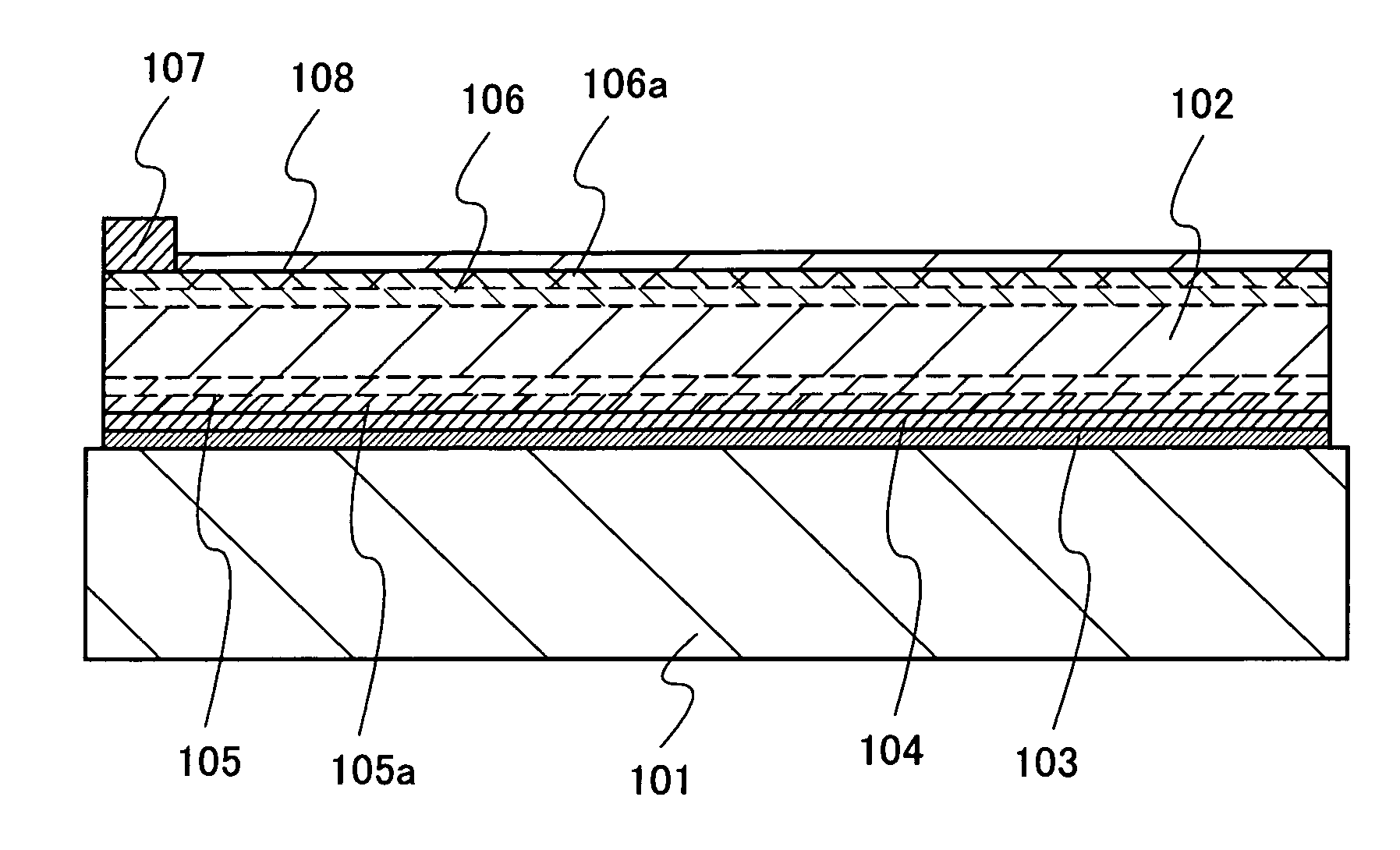
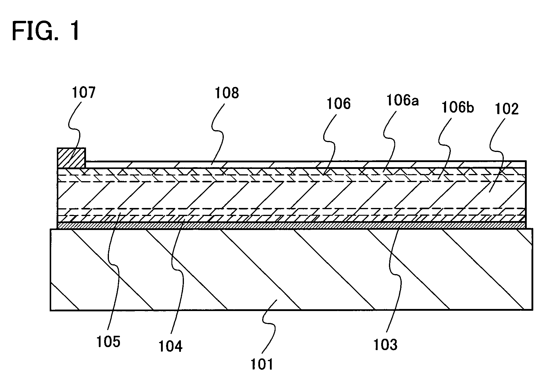
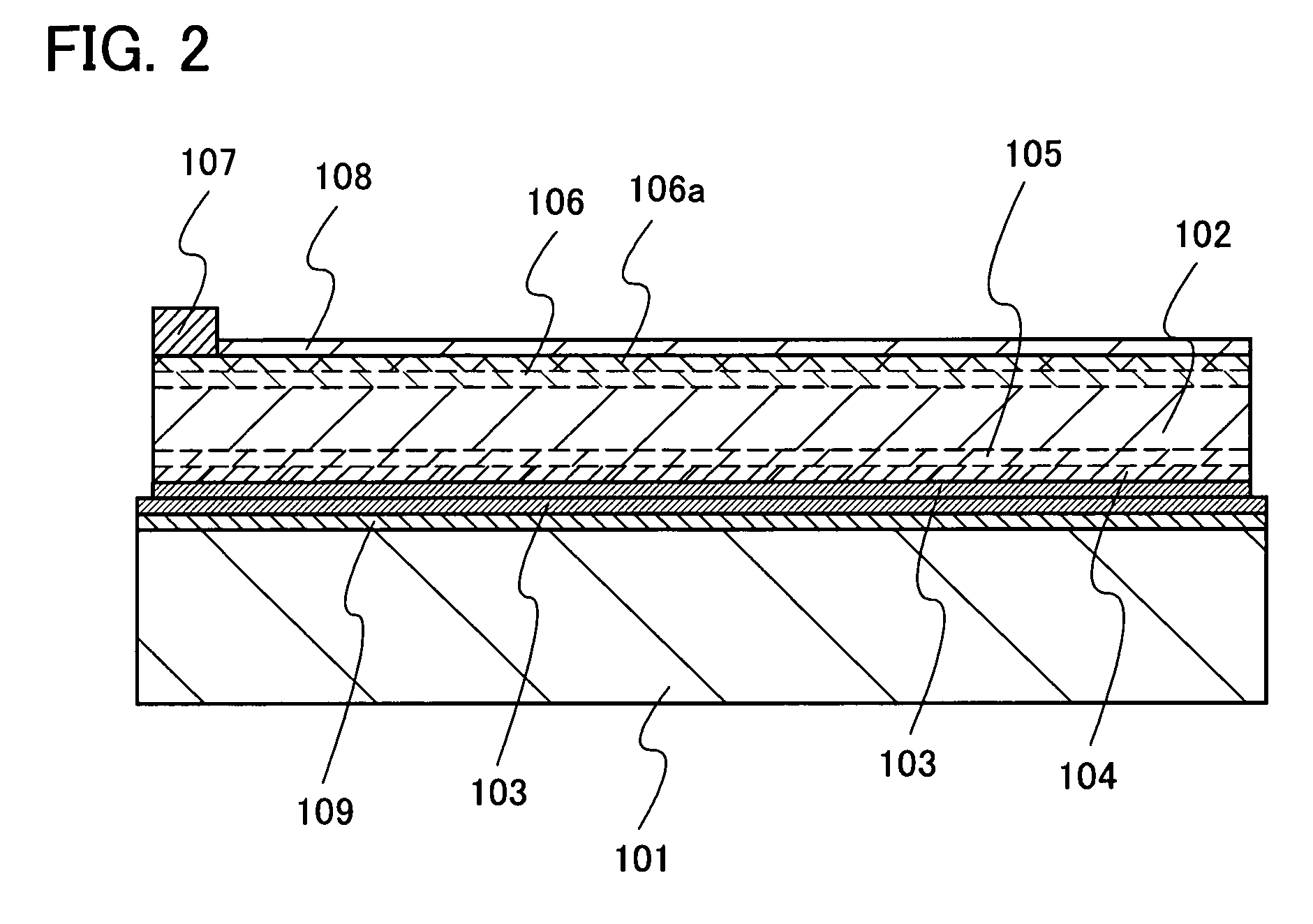
[0057]FIG. 4 is a plan view of a photovoltaic device relating to this embodiment mode. This photovoltaic device has a structure in which light is incident on the semiconductor layer 102 side provided over the substrate 101. In a peripheral portion of the substrate 101, an insulating layer 110 having an opening is provided over the semiconductor layer 102. The second electrode 107 having a comb shape is formed over the semiconductor layer 102. An extraction electrode 111 which is on a side opposite to the second electrode 107 is electrically connected to a first electrode through a contact hole penetrating the insulating layer 110 and the s...

embodiment mode 2

[0077]This embodiment mode describes an example of a method for providing a single crystal semiconductor layer over a large-area substrate and manufacturing a photovoltaic device module. Manufacturing steps of a photovoltaic device is similar to those illustrated in FIGS. 5A to 8C.

[0078]The single crystal semiconductor substrate 112 which is manufactured through the steps in FIGS. 5A to 5D is bonded to the substrate 101. Here, a substrate having an area to which a plurality of the single crystal semiconductor substrates 112 can be bonded is used as the substrate 101. The single crystal semiconductor substrate 112 is fixed to the substrate 101 with the bonding layer 103. A plurality of the single crystal semiconductor substrates 112 are fixed to the substrate 101, and then thermal treatment may be performed thereon to form a bond. When the single crystal semiconductor substrates 112 are separated, the semiconductor layer 102 is disposed over the substrate 101. FIG. 11 shows a state i...

embodiment mode 3

[0083]This embodiment mode describes manufacturing steps for manufacturing a photovoltaic device as described in Embodiment Mode 1, by reusing the single crystal semiconductor substrate 112 from which the semiconductor layer 102 has been taken out.

[0084]FIG. 17A shows a step in which the surface protection film 113 is formed over the single crystal semiconductor substrate 112 which has been used for forming the semiconductor layer 102 in Embodiment Mode 1, and the separation layer 114 is formed by introducing ions of hydrogen or halogen typified by fluorine. Ions of a rare gas such as helium, argon, or krypton may be added to the separation layer 114. The wide band-gap layer 116 remains on a surface side in the single crystal semiconductor substrate 112. The wide band-gap layer 116 is a layer which has been formed as a separation layer in a previous process and which includes hydrogen or halogen which remains in this process. In this process, a surface of the single crystal semicond...


PUM


Abstract

A photovoltaic device uses a single crystal or polycrystalline semiconductor layer which is separated from a single crystal or polycrystalline semiconductor substrate as a photoelectric conversion layer and has a SOI structure in which the semiconductor layer is bonded to a substrate having an insulating surface or an insulating substrate. A single crystal semiconductor layer which is a separated surface layer part of a single crystal semiconductor substrate and is transferred is used as a photoelectric conversion layer and includes an impurity semiconductor layer to which hydrogen or halogen is added on a light incidence surface or on an opposite surface. The semiconductor layer is fixed to a substrate having an insulating surface or an insulating substrate.

Description

TECHNICAL FIELD[0001]The present invention relates to crystal silicon photovoltaic devices and a method for manufacturing crystal silicon photovoltaic devices. The present invention generally relates to photovoltaic devices utilizing photoelectric conversion characteristics of crystalline semiconductors and a method for manufacturing the photovoltaic devices.BACKGROUND ART[0002]As a measure against global warming, solar photovoltaic systems are increasingly installed at many places. The total production of photovoltaic devices in the world in 2005 was 1,759 MW, which is an increase by 147% over the previous fiscal year. At present, the most popular photovoltaic device is crystal photovoltaic devices, and photovoltaic devices using single crystal silicon or polycrystalline silicon account for the large part of the production. A photovoltaic device which is called a crystal photovoltaic device uses a silicon wafer as a base, which is formed by forming a large silicon ingot and slicing...

Claims


Application Information

Patent Timeline
Patent Type & Authority Patents(United States)
IPC IPC(8): H01L31/00H01L21/00
CPCH01L31/0392H01L31/18H01L31/068Y02E10/547H01L31/04
Inventor YAMAZAKI, SHUNPEIARAI, YASUYUKI
Owner SEMICON ENERGY LAB CO LTD
Why Eureka
Try Eureka