

GaN-based semiconductor element
a semiconductor element and gan technology, applied in the field of gan-based semiconductor elements, can solve the problems of increasing resistance and element breaking, and achieve the effect of suppressing the current collaps
- Summary
- Abstract
- Description
- Claims
- Application Information
AI Technical Summary
Benefits of technology
Problems solved by technology
Method used
Image

Examples
first embodiment
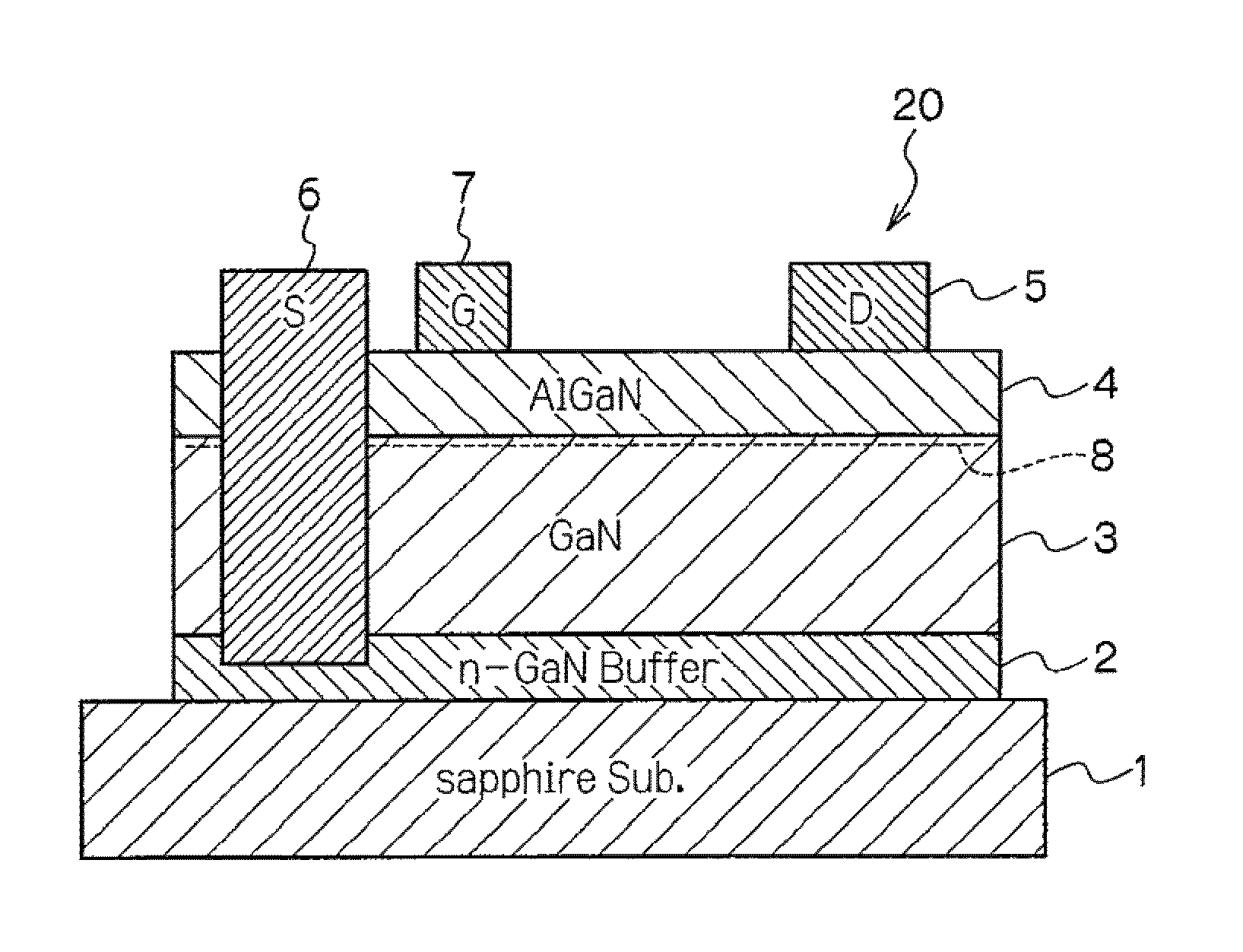
[0018]A GaN-based semiconductor element 20 according to the first embodiment of the present invention will be described in detail below, based on FIG. 1.
[0019]The GaN-based semiconductor element 20 is to be a GaN-based high electron mobility transistor (HEMT) as a GaN-based heterojunction field effect transistor (FET).
[0020]Such the GaN-based semiconductor element 20 comprises a buffer layer 2 formed on a sapphire (0001) substrate 1, a channel layer (an electron transport layer) 3 comprised of a undoped GaN layer on the buffer layer 2, and an electron supply layer 4 comprised of a undoped AlGaN layer formed on the channel layer 3. Moreover, the GaN-based semiconductor element 20 comprises a gate electrode (G) 7, a source electrode (S) 6 and a drain electrode (D) 5 formed on the electron supply layer 4 respectively.
[0021]In such the GaN-based semiconductor element 20, a two-dimensional electron gas 8 is generated at an interface between the channel layer 3 and the electron supply lay...
second embodiment
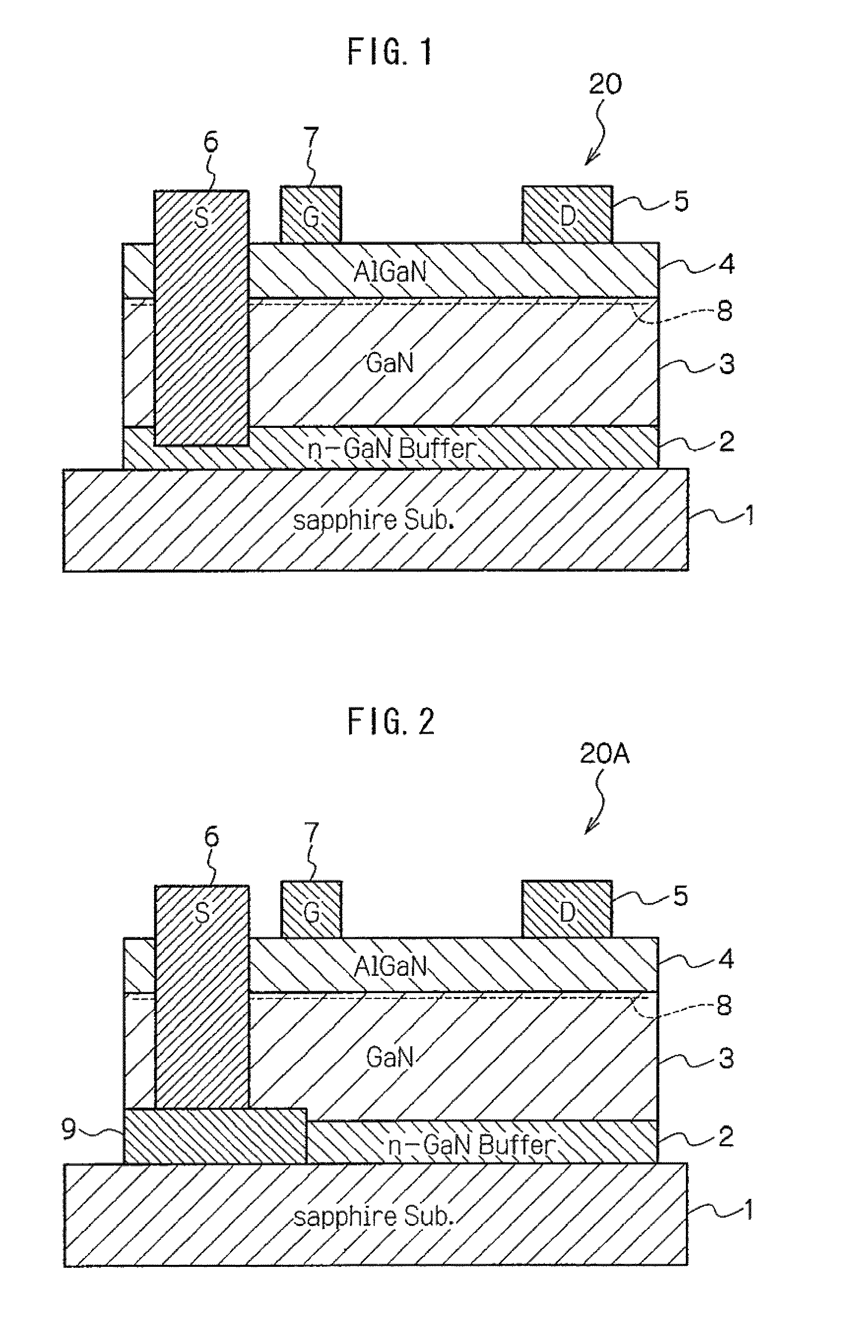
[0039]Next, a GaN-based semiconductor element 20A according to the second embodiment of the present invention will be described in detail below, based on FIG. 2.
[0040]An aspect of such the GaN-based semiconductor element 20A is that the following structure is to be adopted as a structure to be able to control an electric potential of a buffer layer 2 comprised of an n-GaN layer.
[0041]That is to say, in the structure to be able to control the electric potential of the buffer layer 2, there is provided a metal layer 9, which is selectively formed at a part except a region for forming the buffer layer 2 on a sapphire (0001) substrate 1, and which is ohmic contacted to the buffer layer 2. Moreover, the structure includes a configuration that a source electrode 6 is implanted into epitaxial layers (a channel layer 3 and an electron supply layer 4) formed on the buffer layer 2 and the metal layer 9, and that the source electrode 6 is extended to a depth reaching the metal layer 9 for elec...
third embodiment
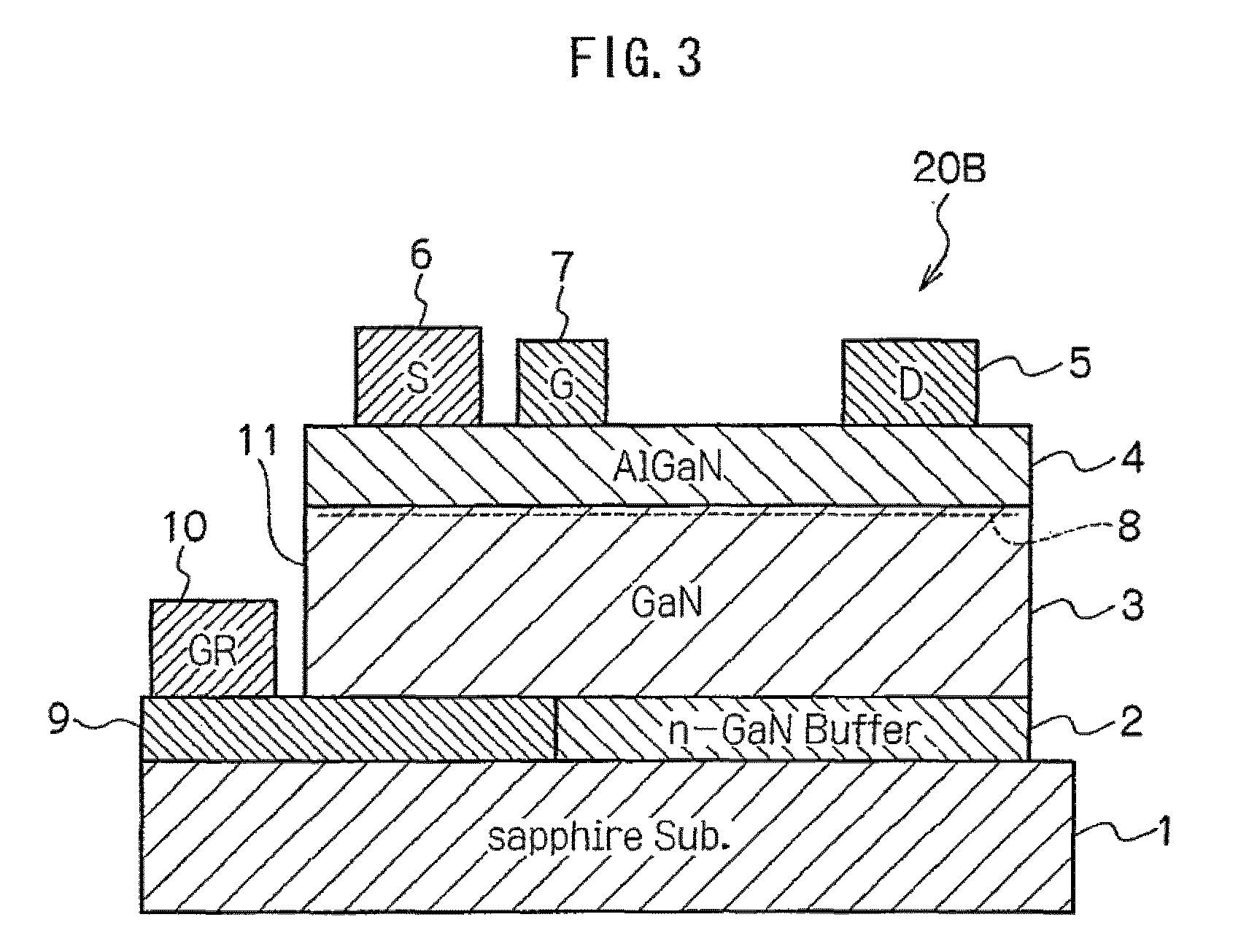
[0051]Next, a GaN-based semiconductor element 20B according to the third embodiment of the present invention will be described in detail below, based on FIG. 3.
[0052]An aspect of such the GaN-based semiconductor element 20B is that the following structure is to be adopted as a structure to be able to control an electric potential of a buffer layer 2 comprised of an n-GaN layer.
[0053]That is to say, in the structure to be able to control the electric potential of the buffer layer 2, there is provided a metal layer 9, which is selectively formed on a part except a region for forming the buffer layer 2 on a sapphire (0001) substrate 1, and which is ohmic contacted to the buffer layer 2. Moreover, the structure includes a configuration that a mesa structure 11 is formed at a part of epitaxial layers (a channel layer 3 and an electron supply layer 4) formed on the buffer layer 2 to be deep for reaching the metal layer 9, and that an electrode 10 is formed on a part of a top surface of th...
PUM
 Abstract
Description
Claims
Application Information