Semiconductor device and preparation method thereof

A technology for semiconductors and devices, applied in the field of semiconductor devices and their preparation, can solve the problems of increased on-resistance, decreased device performance, decreased device transconductance, etc., and achieves the effect of suppressing current collapse and reducing resistance

Pending Publication Date: 2022-07-29
HUAWEI DIGITAL POWER TECH CO LTD
View PDF0 Cites 0 Cited by
  • Summary
  • Abstract
  • Description
  • Claims
  • Application Information

AI Technical Summary

Problems solved by technology

refer to figure 1 , the current collapse manifests as an increase in the on-resistance, a decrease in the transconductance of the device, and a decrease in the output current, which in turn leads to a decrease in the performance of the device.

Method used


Image

  • Semiconductor device and preparation method thereof
  • Semiconductor device and preparation method thereof
  • Semiconductor device and preparation method thereof

Examples


Embodiment Construction

[0047] The technical solutions in the embodiments of the present application will be described below with reference to the accompanying drawings. Obviously, the described embodiments are only a part of the embodiments of the present application, but not all of the embodiments.

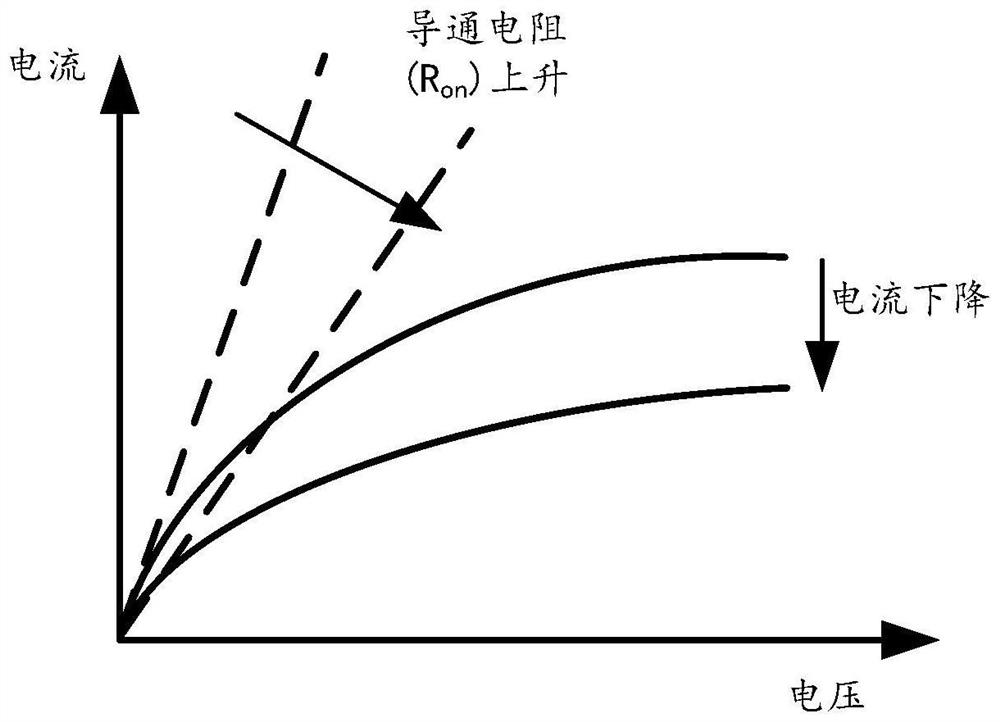
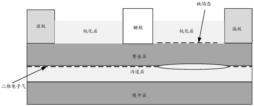
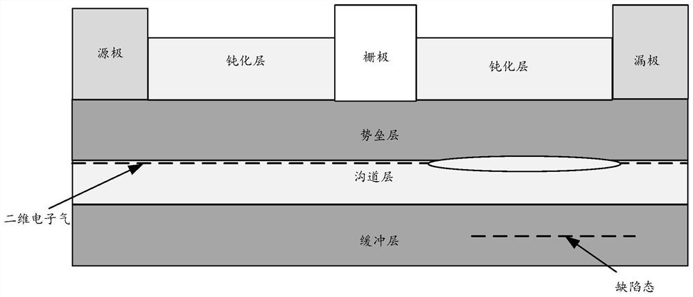
[0048] Current collapse is usually caused by traps in the material. Specifically, when the periodic arrangement of crystal-forming atoms in the crystalline material is disrupted, or when the crystalline material is doped with impurities, defect states can appear in the crystalline material.

[0049] For a typical GaN device such as a GaN-based high electron mobility transistor (HEMT), when it is electrically stressed (wherein the HEMT is on or off, the drain has a voltage ), defect states near the channel region can trap and bind negative charges. These negative charges lower the potential of the channel region, resulting in partial or complete depletion of the two-dimensional electron gas (2DEG) in ...


PUM


Abstract

The invention relates to the technical field of electronic devices, in particular to a semiconductor device and a preparation method thereof, and the semiconductor device comprises a substrate; a P-type semiconductor layer on the substrate; the buffer layer is positioned on the P-type semiconductor layer and is in contact with the P-type semiconductor layer; the channel layer is positioned on the buffer layer; the barrier layer is positioned on the channel layer; and a source electrode, a grid electrode and a drain electrode, wherein the P-type semiconductor layer is connected with the source electrode. The semiconductor device can effectively inhibit current collapse and maintain stable performance.

Description

technical field [0001] The present application relates to the technical field of electronic devices, and in particular, to a semiconductor device and a preparation method thereof. Background technique [0002] A semiconductor device is an electronic device whose conductivity is between a good conductor and an insulator, and uses the special electrical properties of semiconductor materials to complete specific functions. Semiconductor devices have the purposes of generating, controlling, receiving, transforming, amplifying signals, and converting energy. Therefore, semiconductor devices are widely used in many fields. For example, in the field of wireless communication, semiconductor devices can be used as power amplifiers (PAs). In the field of wireless charging, semiconductor devices can be used as power devices for power adapters. [0003] As a third-generation semiconductor device, gallium nitride (gallium nitride, GaN) devices have the properties of large band gap and ...

Claims


Application Information

Patent Timeline
IPC IPC(8): H01L29/06H01L29/778H01L21/335
CPCH01L29/0684H01L29/778H01L29/66462
Inventor 林威沈剑飞
Owner HUAWEI DIGITAL POWER TECH CO LTD
Why Eureka
Try Eureka