Semiconductor substrate and semiconductor element

一种半导体、基板的技术,应用在半导体器件、半导体/固态器件制造、电气元件等方向,能够解决劣化、浓度充分下降、电流坍塌再现性等问题,达到提高结晶性、抑制电流坍塌的发生、降低漏泄电流的效果

Active Publication Date: 2016-12-14
SANKEN ELECTRIC CO LTD +1
View PDF8 Cites 1 Cited by
  • Summary
  • Abstract
  • Description
  • Claims
  • Application Information

AI Technical Summary

Problems solved by technology

[0005] On the other hand, if the upper layer of the GaN layer functions as a channel layer and forms a level for trapping carriers, it may become the main cause of current collapse (a phenomenon in which the reproducibility of output current characteristics deteriorates), Therefore, the concentration of carbon and the like must be sufficiently reduced (see Patent Documents 1-3)

Method used


Image

  • Semiconductor substrate and semiconductor element
  • Semiconductor substrate and semiconductor element
  • Semiconductor substrate and semiconductor element

Examples


Embodiment 1

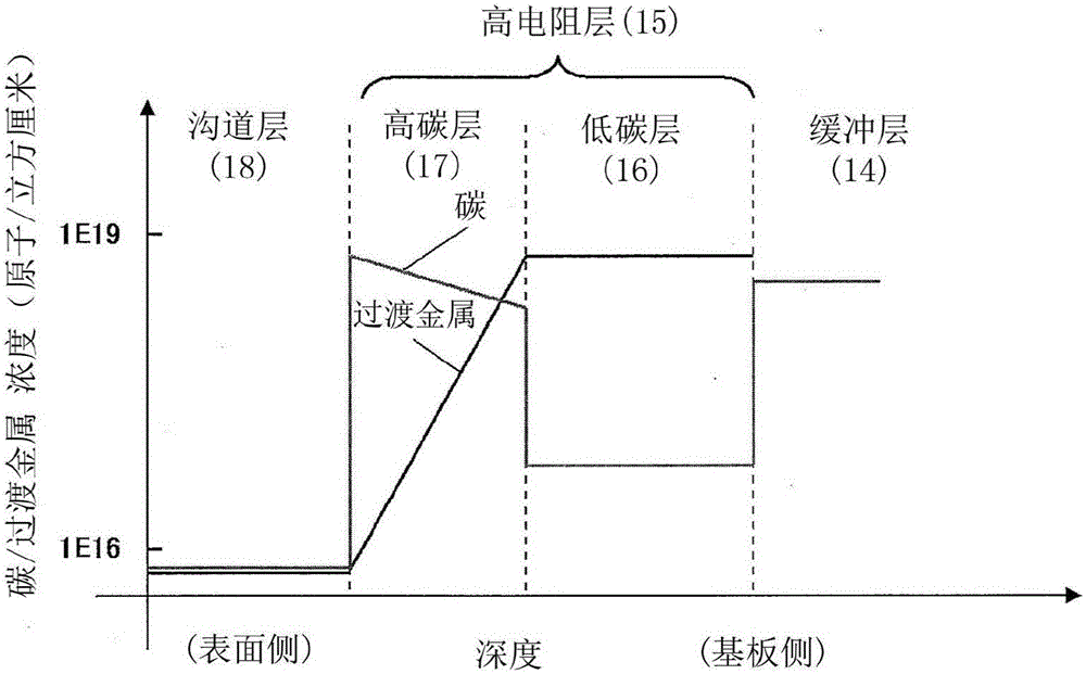
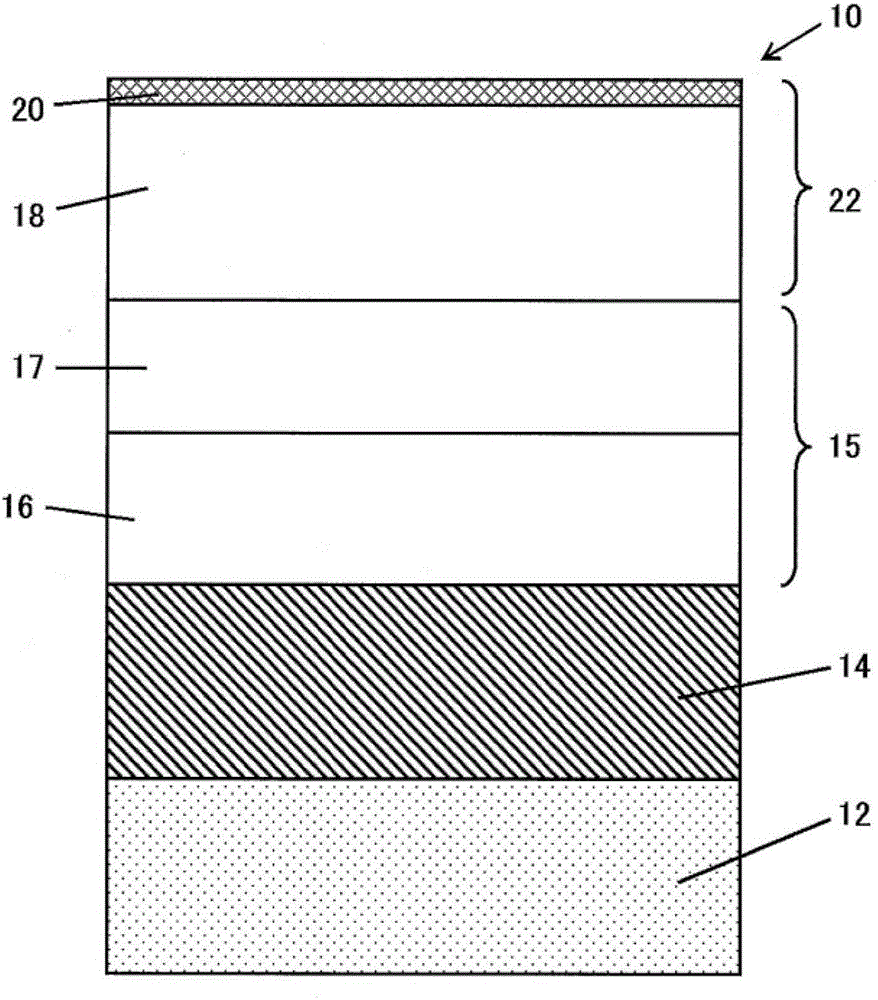
[0087] make figure 2 The semiconductor substrate shown, the semiconductor substrate has figure 1 The concentration distribution in the depth direction is shown. However, using Fe as the transition metal, the carbon concentration in the low carbon layer 16 is set to 5×10 17 Atoms / cm3, the carbon concentration in the high carbon layer 17 is set to 2×10 18 Atoms / cm3, the concentration of Fe in the low carbon layer 16 is set to 3×10 18 atoms / cubic centimeter. In addition, the thickness of the low carbon layer 16 was set to 500 nm, and the thickness of the high carbon layer was set to 1600 nm.

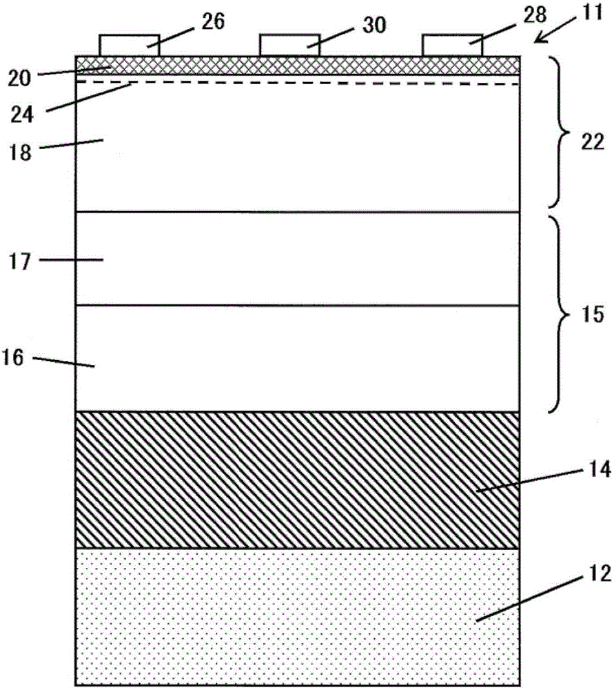
[0088] Using the fabricated semiconductor substrates, such as image 3 semiconductor components shown.

Embodiment 2

[0090] make figure 2 The semiconductor substrate shown, the semiconductor substrate has Figure 4 The concentration distribution in the depth direction is shown. However, the transition metal was not added to the high-resistance layer 15, and the carbon concentration in the low-carbon layer 16 was set to 3×10 17 Atoms / cm3, the carbon concentration in the high carbon layer 17 is set to 2×10 18 atoms / cubic centimeter. In addition, the thickness of the low carbon layer 16 was set to 100 nm, and the thickness of the high carbon layer was set to 1600 nm.

[0091] Using the fabricated semiconductor substrates, such as image 3 semiconductor components shown.

Embodiment 3

[0093] A semiconductor substrate was produced in the same manner as in Example 2. However, the thickness of the low carbon layer 16 was set to 200 nm, and the thickness of the high carbon layer 17 was set to 1500 nm.

[0094]The crystallinity of the GaN layer (including the high carbon layer 17 ) in the 0002 direction on the low carbon layer 16 was measured using X-ray diffraction for the fabricated semiconductor substrate. display the results in Figure 8 middle.

[0095] Using the fabricated semiconductor substrates, such as image 3 semiconductor components shown.


PUM


Abstract

A semiconductor substrate of the present invention has: a substrate; a buffer layer on the substrate, said buffer layer being formed of a carbon-containing nitride semiconductor; a high-resistance layer on the buffer layer, said high-resistance layer being formed of a carbon-containing nitride semiconductor; and a channel layer on the high-resistance layer, said channel layer being formed of a nitride semiconductor. The semiconductor substrate is characterized in that the high-resistance layer has: a first region having a carbon concentration lower than that of the buffer layer; and a second region, which is provided between the first region and the channel layer, and which has a carbon concentration higher than that of the first region. Consequently, a leak current is reduced by improving crystallinity, while maintaining the high resistance of the high-resistance layer, and crystallinity of the channel layer formed on the high-resistance layer is also increased, thereby providing the semiconductor substrate wherein deterioration of electron mobility and generation of current collapse in the channel layer are suppressed.

Description

technical field [0001] The present invention relates to a semiconductor substrate and a semiconductor element, and the semiconductor element is fabricated using the semiconductor substrate. Background technique [0002] Semiconductor substrates using nitride semiconductors have been used for power elements and the like that operate at high frequencies and high outputs. In particular, as a power element suitable for amplifying in high frequency bands such as microwaves, submillimeter waves, and millimeter waves, for example, high electron mobility transistors (HEMTs) and the like are known. [0003] As a semiconductor substrate using a nitride semiconductor, a semiconductor substrate is known in which a buffer layer, a GaN (gallium nitride) layer, and a barrier layer composed of AlGaN (aluminum gallium nitride) are formed on a Si (silicon) substrate in accordance with the Sequentially layered. [0004] The lower layer (high-resistance layer) of the GaN layer can improve the...

Claims


Application Information

Patent Timeline
Patent Type & Authority Applications(China)
IPC IPC(8): H01L21/338H01L29/778H01L29/812
CPCH01L21/02378H01L21/0242H01L21/02458H01L21/0254H01L21/02579H01L21/0262H01L29/2003H01L29/207H01L29/66462H01L29/7786H01L21/2003
Inventor 佐藤宪鹿内洋志后藤博一篠宫胜萩本和德土屋庆太郎
Owner SANKEN ELECTRIC CO LTD
Why Eureka
Try Eureka