Connector assembly having adjacent differential signal pairs offset or of different polarity

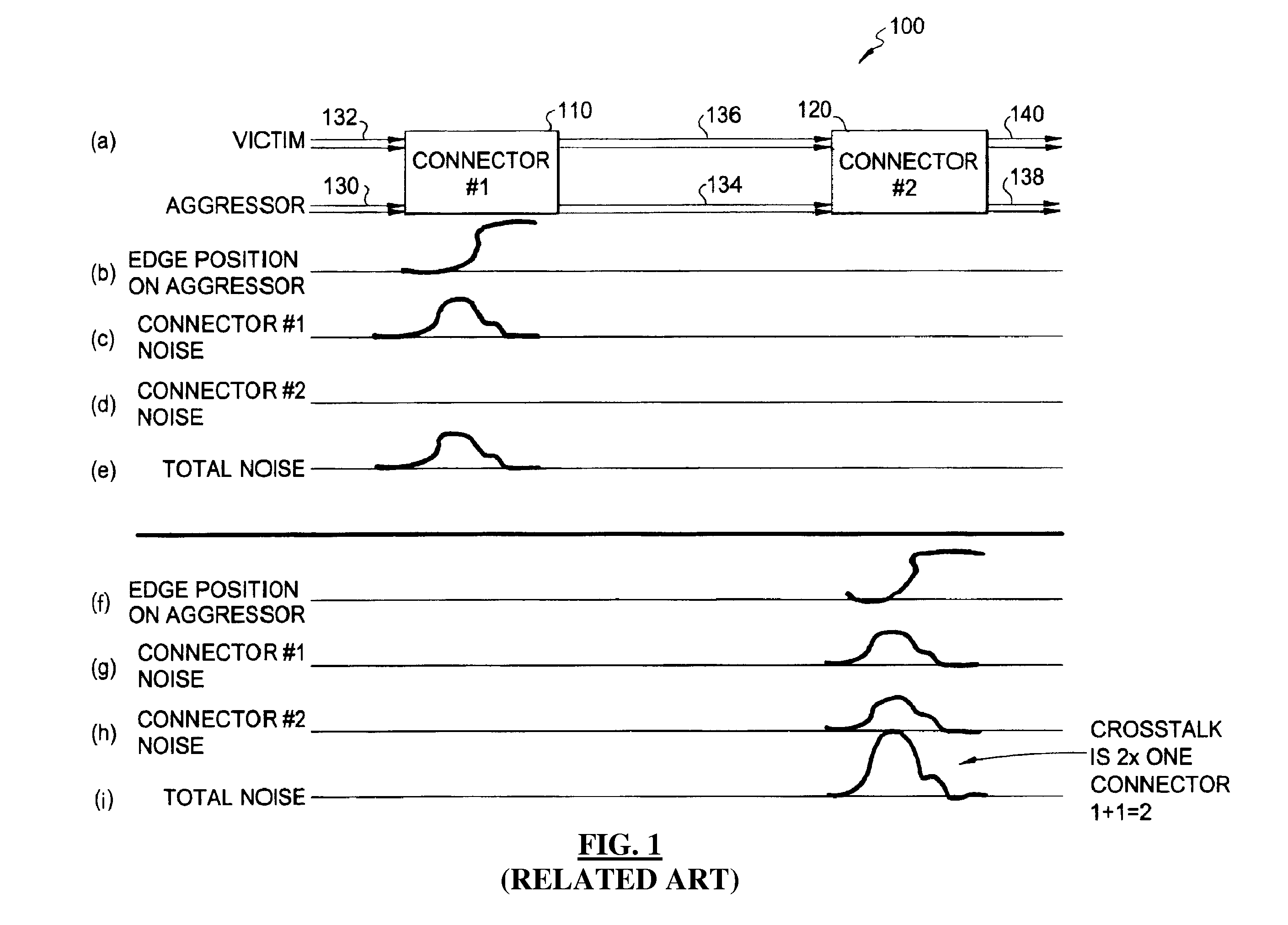
a technology of differential signal pairs and connecting assemblies, which is applied in the direction of orthogonal pcbs mounting, coupling device connection, printed circuit aspects, etc., can solve the problems of increasing electrical noise between signal conductors, increasing the possibility of energy loss, and increasing the problem of electrical noise between signals

Active Publication Date: 2012-07-10
AMPHENOL CORP
View PDF22 Cites 44 Cited by
  • Summary
  • Abstract
  • Description
  • Claims
  • Application Information

AI Technical Summary

Problems solved by technology

As a result of the increased density of traces, electrical noise between signals has become more problematic.
Electrical noise is usually considered any undesirable electrical energy in an electronic system, including but not limited to reflections, electromagnetic interference, mode conversions, and unwanted coupling, such as crosstalk.
A major difficulty with placing signal conductors closer together is that electrical noise between the signal conductors increases as the distance between signal conductors decreases and as the speed of the signals increases.
In addition, as frequency content increases, there is a greater possibility of energy loss.
Energy loss may be attributed to impedance discontinuities, mode conversion, leakage from imperfect shielding, or undesired coupling to other signal conductors, such as crosstalk.
At high speeds, the available conducting paths may encounter crosstalk, impedance, and attenuation mismatch characteristics, and the signal transmission characteristics may degrade.
Those via cylinders can also couple to each other and generate noise.
While it is possible to minimize those deleterious coupling effects by adding space between the victim and aggressor lines, that comes at the disadvantage of losing density in the backplane and the connector.
Thus, as more and more signals are populated onto backplanes and more and more signal conductors are provided in connectors, the problem with coupling becomes more probable and more problematic.

Method used


Image

  • Connector assembly having adjacent differential signal pairs offset or of different polarity
  • Connector assembly having adjacent differential signal pairs offset or of different polarity
  • Connector assembly having adjacent differential signal pairs offset or of different polarity

Examples


Embodiment Construction

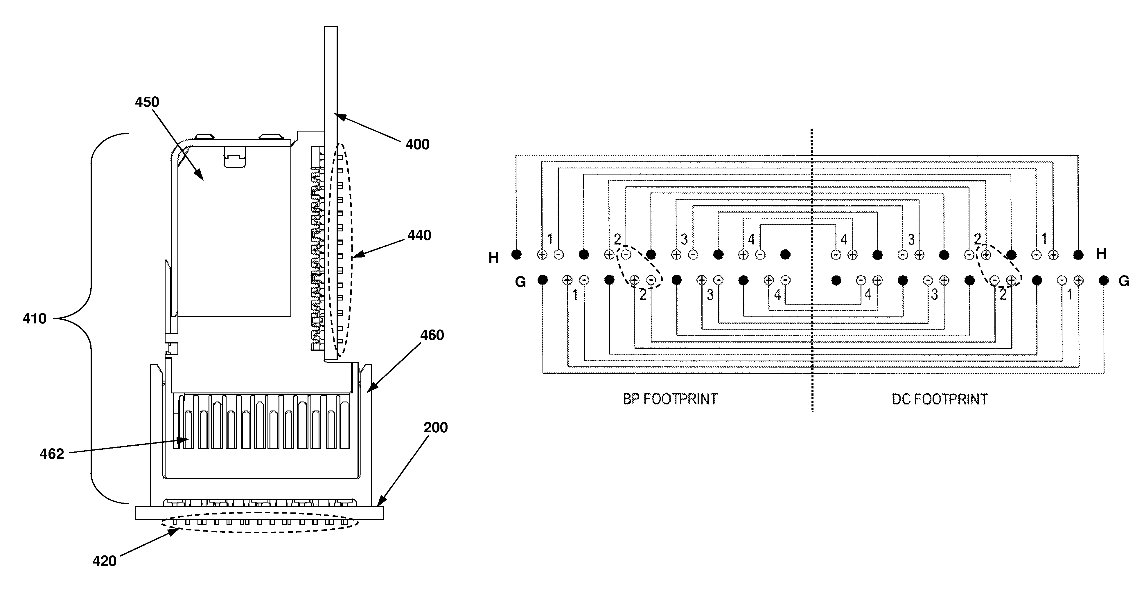
[0024]In describing the preferred embodiments of the invention illustrated in the drawings, specific terminology will be resorted to for the sake of clarity. However, the invention is not intended to be limited to the specific terms so selected, and it is to be understood that each specific term includes all technical equivalents that operate in a similar manner to accomplish a similar purpose.

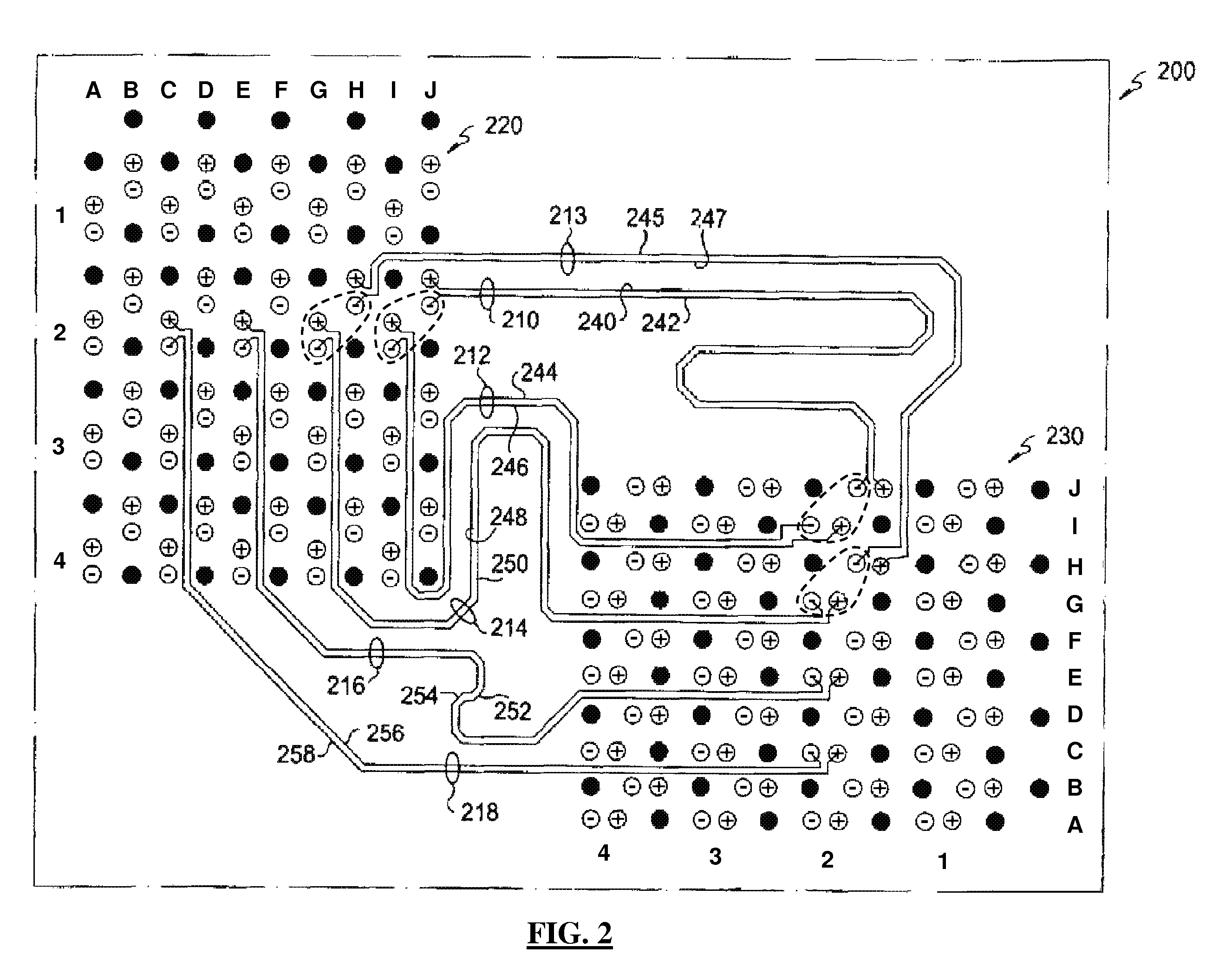
[0025]Turning to the drawings, FIG. 2 shows a backplane 200 having a first footprint 220 and a second footprint 230 in accordance with a non-limiting embodiment of the present invention. The first footprint 220 and the second footprint 230 each have a plurality of signal launches, shown in FIG. 2 as an array of ten columns (A-J) each having four rows (1-4) of differential signal pairs. Each differential signal pair includes a launch that carries the positive “+” signal (P) of the differential signal pair and a launch that carries the negative “−” signal (N) of the differential signal pair. The...


PUM

PropertyMeasurementUnit
lengthaaaaaaaaaa
lengthaaaaaaaaaa
lengthaaaaaaaaaa

Abstract

A connector for connecting a first printed circuit board with a second printed circuit board that comprises a first column of differential signal pair launches offset from a second column of differential signal pair launches on the first printed circuit board so that each differential signal pair in the first column is closest to a launch of a first polarity in a corresponding differential signal pair in the second column on the first circuit board, a first column of differential signal pair launches offset from a second column of differential signal pair launches on the second printed circuit board so that each differential signal pair in the first column is closest to a launch of a second polarity, opposite the first polarity, in a corresponding signal pair in the second column on the second circuit board, and a connector electrically connecting the first column of differential signal pair launches on the first printed circuit board to the first column of differential signal pair launches on the second printed circuit board and electrically connecting the second column of differential signal pair launches on the first printed circuit board to the second column of differential signal pair launches on the second printed circuit board.

Description

CROSS-REFERENCE TO RELATED APPLICATION[0001]The present patent application claims the benefit of U.S. Provisional Application Ser. No. 61 / 300,387, filed Feb. 1, 2010, and is related to U.S. Pat. No. 7,607,951, filed Jan. 16, 2009, the entire disclosures of which are incorporated herein by reference.BACKGROUND OF THE INVENTION[0002]1. Field of the Invention[0003]The present invention relates to a system for reducing noise in a backplane system. More particularly, the present invention reverses pin connections between backplanes to reduce crosstalk generated between pin connections in the backplanes.[0004]2. Background of the Related Art[0005]Electronic systems are often assembled from multiple printed circuit boards (PCBs). PCBs that contain electronic components are sometimes called “daughter cards.” Often, electrical signals are routed from one daughter card to another through a PCB called a “backplane.” A backplane includes conducting paths called “signal traces,” or just “traces,...

Claims


Application Information

Patent Timeline
Patent Type & Authority Patents(United States)
IPC IPC(8): H01R24/00
CPCH05K1/0228H01R13/6469H05K1/0245H05K2201/044H05K2201/09236H05K2201/09263Y10T29/49117H01R13/6587H05K2201/09227H05K2201/10189
Inventor KIRK, BRIAN PETER
Owner AMPHENOL CORP
Why Eureka
Try Eureka