Integrated circuit packaging system with quad flat no-lead package and method of manufacture thereof

a technology of integrated circuit packaging and no lead package, which is applied in the direction of electrical apparatus, semiconductor devices, semiconductor/solid-state device details, etc., can solve the problems of long time-consuming and laborious, inability to fully address the requirements of lower height, cost reduction, and small space, and achieves the effects of reducing labor intensity, reducing labor intensity, and reducing labor intensity

Active Publication Date: 2012-12-18
STATS CHIPPAC LTD
View PDF21 Cites 12 Cited by
  • Summary
  • Abstract
  • Description
  • Claims
  • Application Information

AI Technical Summary

Problems solved by technology

While these approaches provide more functions within an integrated circuit, they do not fully address the requirements for lower height, smaller space, and cost reduction.
Solutions to these problems have been long sought but prior developments have not taught or suggested any solutions and, thus, solutions to these problems have long eluded those skilled in the art.

Method used


Image

  • Integrated circuit packaging system with quad flat no-lead package and method of manufacture thereof
  • Integrated circuit packaging system with quad flat no-lead package and method of manufacture thereof
  • Integrated circuit packaging system with quad flat no-lead package and method of manufacture thereof

Examples


first embodiment

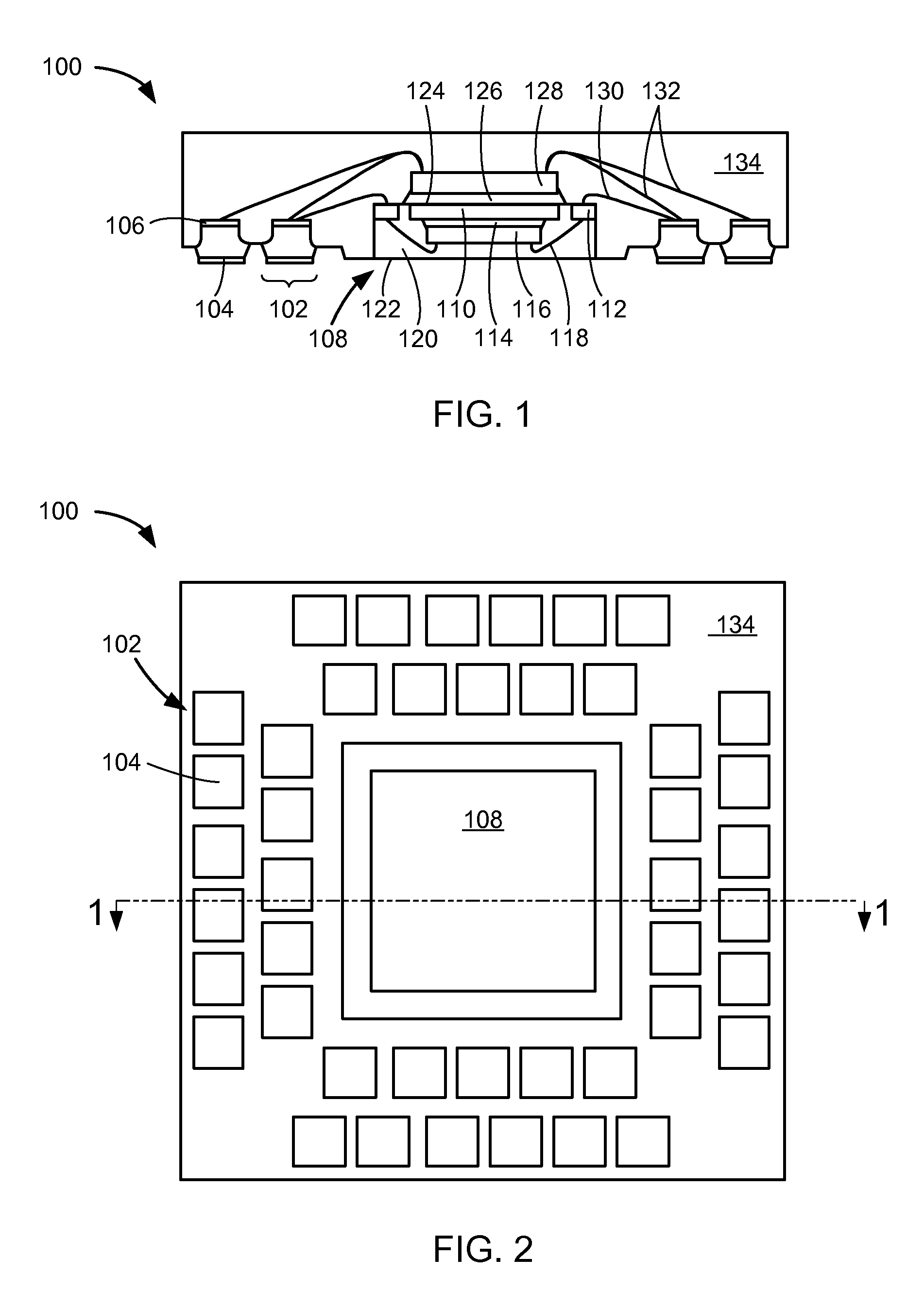
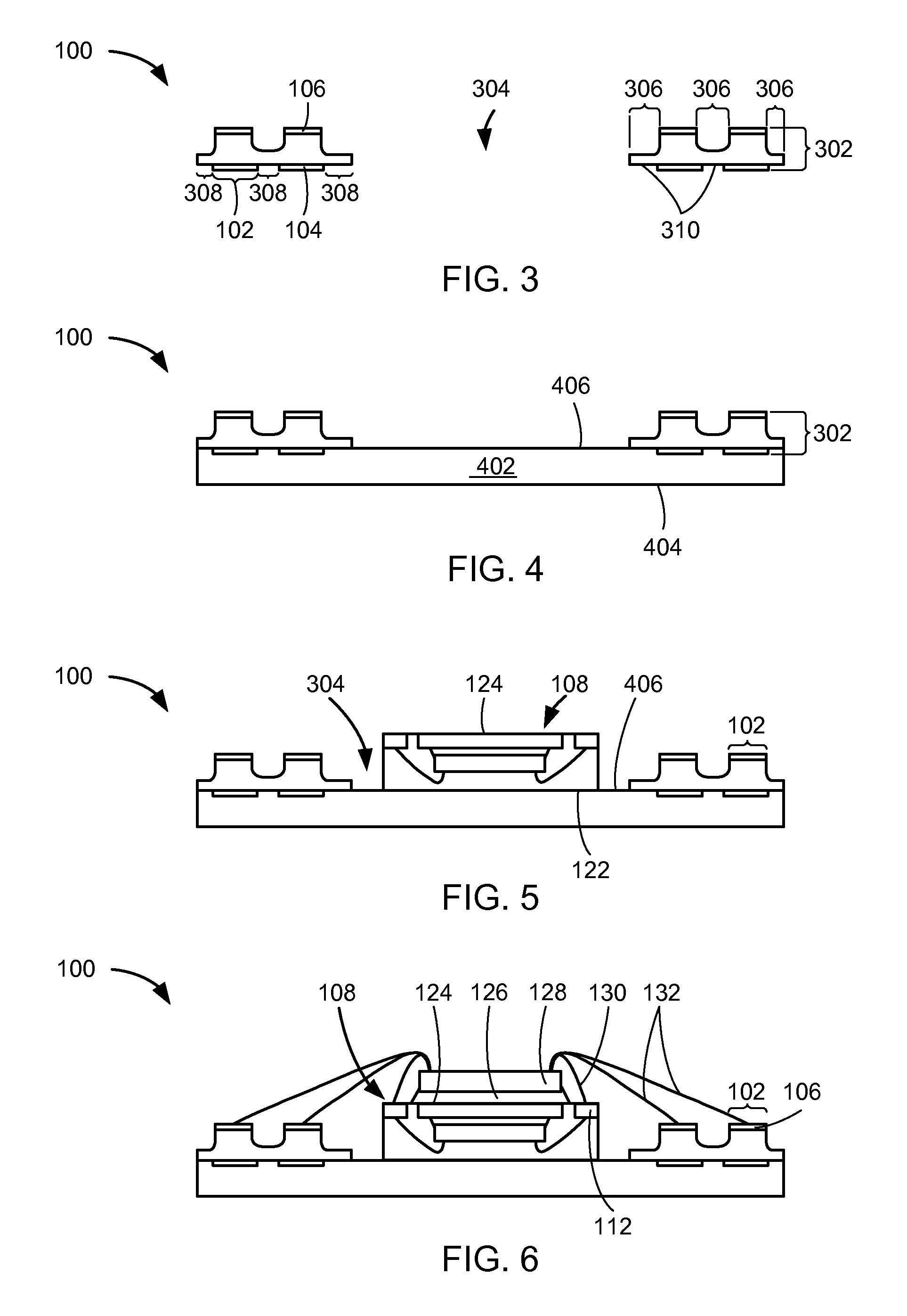
[0032]Referring now to FIG. 1, therein is shown a cross-sectional view of an integrated circuit packaging system 100 along a section line 1-1 of FIG. 2 in the present invention. The integrated circuit packaging system 100 can include a package, a multi-row quad flat no-lead (QFN-mr) package, a package-in-package QFN-mr package, a saw singulated QFN-mr (QFNs-mr) package, or a tapeless quad flat no-lead (QFN) package.

[0033]The integrated circuit packaging system 100 can include a terminal 102, such as a terminal lead or a peripheral lead of a leadframe, a copper leadframe, or a copper sheet that is etched, stamped, cut, or a combination thereof. The terminal 102 can include an external plated layer 104, such as a layer formed by a backside selective pre-plated leadframe (PPF) plating process, formed at the bottom of the terminal 102 for providing an electrical connection to external systems. The external plated layer 104 can be formed with nickel (Ni), palladium (Pd), gold (Au), or an...

second embodiment

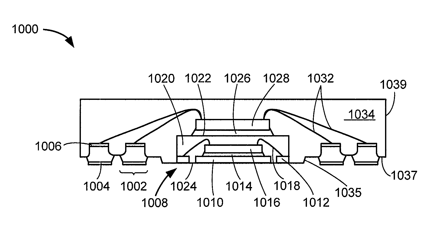
[0072]Referring now to FIG. 10, therein is shown a cross-sectional view similar to FIG. 1 of an integrated circuit packaging system 1000 in the present invention. The integrated circuit packaging system 1000 can include a multi-row quad flat no-lead (QFN-mr) package, a package-in-package QFN-mr package, a saw singulated QFN-mr (QFNs-mr) package, or a tapeless quad flat no-lead (QFN) package.

[0073]The integrated circuit packaging system 1000 can include a terminal 1002, such as a terminal lead or a peripheral lead of a leadframe, a copper leadframe, or a copper sheet that is etched, stamped, cut, or a combination thereof. The terminal 1002 can include an external plated layer 1004, such as a layer formed by a backside selective pre-plated leadframe (PPF) plating process, formed at the bottom of the terminal 1002 for providing an electrical connection to external systems. The external plated layer 1004 can be formed with nickel (Ni), palladium (Pd), gold (Au), or any other conductive ...

third embodiment

[0085]Referring now to FIG. 11, therein is shown a cross-sectional view similar to FIG. 1 of an integrated circuit packaging system 1100 in the present invention. The integrated circuit packaging system 1100 can include a multi-row quad flat no-lead (QFN-mr) package, a thermally enhanced QFN-mr package, a saw singulated QFN-mr (QFNs-mr) package, or a tapeless quad flat no-lead (QFN) package.

[0086]The integrated circuit packaging system 1100 can include a terminal 1102, such as a terminal lead or a peripheral lead of a leadframe, a copper leadframe, or a copper sheet that is etched, stamped, cut, or a combination thereof. The terminal 1102 can include an external plated layer 1104, such as a layer formed by a backside selective pre-plated leadframe (PPF) plating process, formed at the bottom of the terminal 1102 for providing an electrical connection to external systems. The external plated layer 1104 can be formed with nickel (Ni), palladium (Pd), gold (Au), or any other conductive ...


PUM


Abstract

A method of manufacture of an integrated circuit packaging system includes: providing a base array having terminals and an open region; attaching a coverlay layer directly on the base array; placing a component in the open region and directly on the coverlay layer; forming an encapsulation over the base array and the component; removing the coverlay layer to leave a plane of the terminals and a plane of the component partially exposed and substantially coplanar; and removing a portion of the base array between the terminals, the terminals electrically isolated.

Description

TECHNICAL FIELD[0001]The present invention relates generally to an integrated circuit packaging system, and more particularly to a system for an integrated circuit packaging system with quad flat no-lead package.BACKGROUND ART[0002]Modern electronics, such as smart phones, personal digital assistants, location based services devices, enterprise class servers, or enterprise class storage arrays, are packing more integrated circuits into an ever shrinking physical space with expectations for decreasing cost. Numerous technologies have been developed to meet these requirements. Some of the research and development strategies focus on new technologies while others focus on improving the existing and mature technologies. Research and development in the existing technologies can take a myriad of different directions.[0003]Consumer electronics requirements demand more integrated circuits in an integrated circuit package while paradoxically providing less physical space in the system for th...

Claims


Application Information

Patent Timeline
Patent Type & Authority Patents(United States)
IPC IPC(8): H01L23/495H01L21/44
CPCH01L21/4832H01L21/56H01L21/565H01L23/3107H01L23/3114H01L23/3135H01L23/4334H01L23/49541H01L23/49548H01L23/49575H01L23/49582H01L24/48H01L25/03H01L2224/48091H01L2224/48247H01L2224/48257H01L2224/484H01L2224/73265H01L2224/85001H01L2224/85439H01L2224/85444H01L2224/85455H01L2224/85464H01L2924/01028H01L2924/01029H01L2924/01046H01L2924/01047H01L2924/01078H01L2924/01079H01L2924/01082H01L2924/14H01L2924/00014H01L2224/32245H01L2924/00H01L2924/15747H01L2924/181H01L2224/45099H01L2224/05599H01L2924/00012
Inventor CAMACHO, ZIGMUND RAMIREZBATHAN, HENRY DESCALZOESPIRITU, EMMANUEL
Owner STATS CHIPPAC LTD
Why Eureka
Try Eureka