System and method for attenuation of electrical noise

a technology of electrical noise and attenuation method, applied in the field of electrical noise attenuation system, can solve the problem of typical generation of significant noise, and achieve the effect of cancelling common background nois

Inactive Publication Date: 2013-02-05
CHOW VINCENT Y
View PDF10 Cites 0 Cited by
  • Summary
  • Abstract
  • Description
  • Claims
  • Application Information

AI Technical Summary

Benefits of technology

[0010]The Present Invention generally provides a method and system to attenuate electrical noise and background in a monitoring or detecting product, thereby being able to clearly reproduce and illustrate weak target input signals. Background signals in embodiments of the Present Invention are suppressed by what is referred to as “common mode rejection” techniques, that is, by techniques that cancel common mode signals and, here, that cancel common background noise. This noise attenuation is accomplished in the detector and preamplifier stage of a detector system, where significant noise is typically generated. Noise attenuation in embodiments of the Present Invention can be accomplished, and can provide enhanced images, where the target input signal is unknown, is of a transient nature or where there is very little data available to analyze the signal.
[0011]Following the teaching of the Present Invention, the target input signal (which can be any type of input, such as an optical signal or one of vibration, magnetic field, sound, heat, pressure, etc.) is split into two components, preferably through a process called “dither chopping” Each of the two components is then coded, or “tagged,” with a unique marker as the input signal components are converted into an electrical format. The unique encoding technique of the Present Invention maintains full view of the input scene and does not have scene blindness problems caused by physical light shutters used in lock-in and synchronous detection systems. As a consequence, the noise reduction technology in the detection circuit of embodiments of the Present Invention do not suffer from a 50% loss in input signal strength occurring in current “chopper” based systems (e.g., having a physical input shutter), and, therefore, have up to twice the detection sensitivity. Significantly, the random noise, containing white noise and non-white noise, generated in the system electronics in embodiments of the Present Invention is suppressed by lowering the non-white noise with synchronous phase detection and lowering the white noise by enabling reduced bandwidth in operation. In an optical system using the Present Invention, for example, background signals are immediately suppressed at the detector by common mode rejection and the detector system “tagging” each input component with +1 or −1 polarity flags as the signal enters the optical-to-electrical conversion process. The tagged signal components are then synchronized with a second stage of reverse electronic chopping and combined, thereby reestablishing and preserving the original input signal. In this reverse chopping stage, non-white random noise segments are cancelled and the overall electrical noise effectively attenuated. The simultaneous combination of full-signal non-white noise suppression by polarity coding, common mode rejection at the sense node and white noise reduction by narrow bandwidth has never been taught before. The preservation of the original input signal, while attenuating electronic noise, provides an exceptionally clear, relatively noise-free, visual image.

Problems solved by technology

This noise attenuation is accomplished in the detector and preamplifier stage of a detector system, where significant noise is typically generated.

Method used


Image

  • System and method for attenuation of electrical noise
  • System and method for attenuation of electrical noise
  • System and method for attenuation of electrical noise

Examples


Embodiment Construction

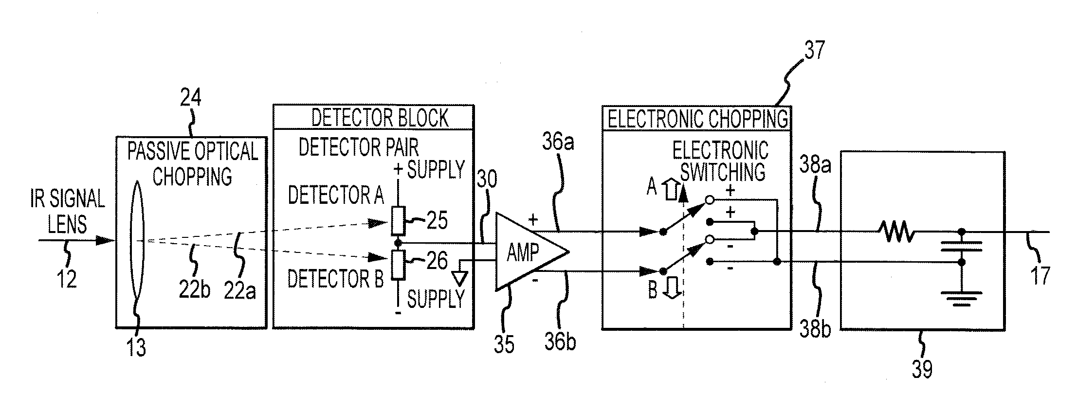
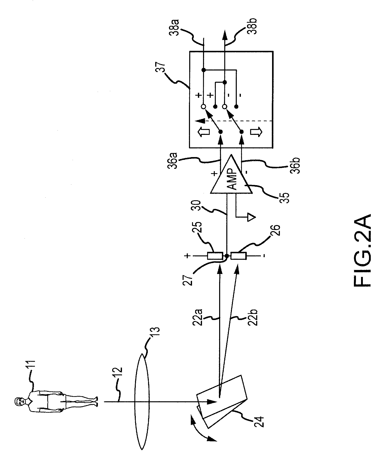
thus include an input signal chopping device to produce at least two input signal components, and at least two detectors or an alternating detector system with opposite polarities to detect the at least two dither chopped input signal components while simultaneously cancelling background signals common to the detectors. Differential signals from the at least two detectors or alternating detector system are then superimposed to create a single detector current signal. A preamplifier is provided to receive that single detector signal, followed by electronic switch means to flip polarity of detected current signal segments, thereby combining and reestablishing the original input. A low pass filter, an amplifier, and an analog-to-digital converter can also be added, resulting in a final digital detection signal.

BRIEF DESCRIPTION OF THE FIGURES

[0013]Features, aspects, and embodiments of the Present Invention are described in conjunction with the attached drawings, in which:
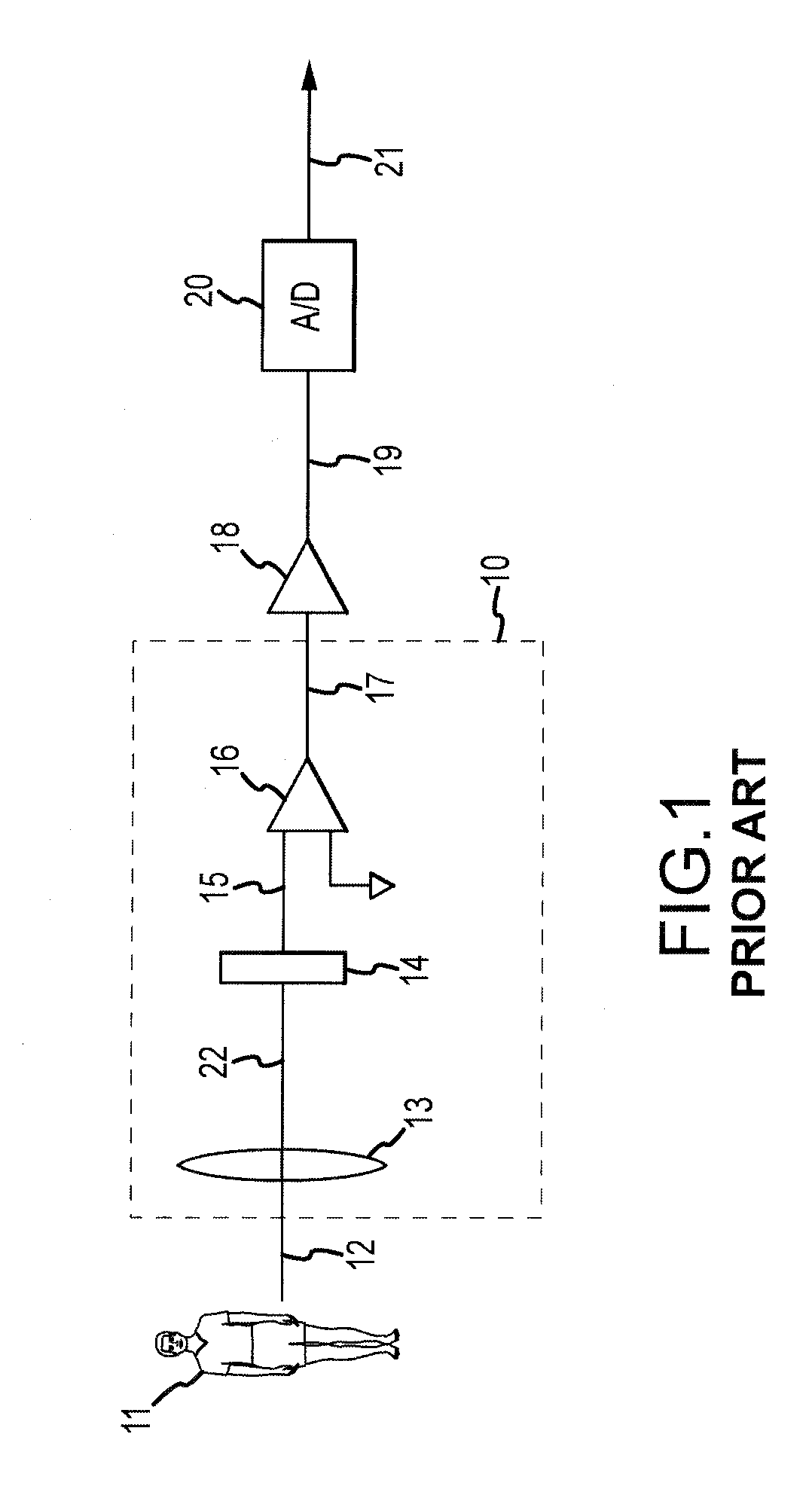
[0014]FIG. 1 i...


PUM


Abstract

The Present Invention relates to methods and systems particularly useful in electrical products used to monitor and detect very weak signals. These products include, for example, night vision binoculars and remote listening devices. More specifically, the methods and systems of the Present Invention provide a signal conditioning technique that attenuates electrical noise generated within the product while at the same time preserving the integrity of the input signal. This provides a high signal-to-noise ratio within the product electronics and a dramatically clear final image. The Present Invention includes a method and system for chopping or splitting an input signal into two components, tagging each of the split signal components with opposite polarities, and a second reverse chopping step that combines the split and tagged input signal components into a restored input signal. The combining step, in addition to restoring the original input signal, cancels and attenuates internally generated, and untagged, electronic noise, providing image quality and detection in an efficient and economical manner that could not be obtained in the past.

Description

CROSS-REFERENCE TO RELATED APPLICATIONS[0001]This application is a continuation-in-part of international application no. PCT / US2008 / 069612, filed 10 Jul. 2008 and published in English on 22 Jan. 2009 under international publication no. WO 2009 / 012106 (the '612 application), which claims the benefit of U.S. provisional application No. 60 / 949,743 filed 13 Jul. 2007 (the '743 application). The '612 application and '743 application are both hereby incorporated by reference as though fully set forth herein.[0002]This Invention was developed with Government support under HQ0006-07-C-7776 awarded by the Missile Defense Agency. The Government may have certain rights in the invention.FIELD OF THE PRESENT INVENTION[0003]The Present Invention relates to electronic methods and systems for the high quality detection and monitoring of very weak signals. More particularly, the Present Invention relates to a signal conditioning method and apparatus for suppressing or attenuating electrical noise wh...

Claims


Application Information

Patent Timeline
Patent Type & Authority Patents(United States)
IPC IPC(8): G01J5/20
CPCH03F3/183H03F3/387
Inventor CHOW, VINCENT Y.
Owner CHOW VINCENT Y
Why Eureka
Try Eureka