[0010]The Present Invention generally provides a method and
system to attenuate electrical noise and background in a monitoring or detecting product, thereby being able to clearly reproduce and illustrate weak target input signals. Background signals in embodiments of the Present Invention are suppressed by what is referred to as “common mode rejection” techniques, that is, by techniques that cancel common mode signals and, here, that cancel common
background noise. This
noise attenuation is accomplished in the
detector and
preamplifier stage of a detector system, where significant noise is typically generated.
Noise attenuation in embodiments of the Present Invention can be accomplished, and can provide enhanced images, where the target input signal is unknown, is of a transient nature or where there is very little data available to analyze the signal.
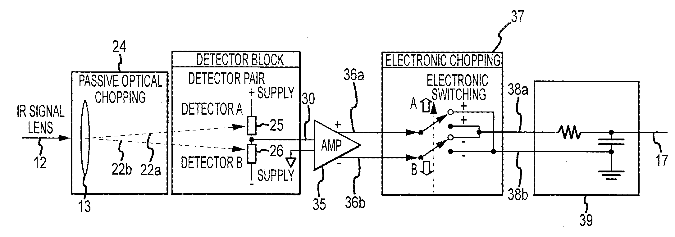
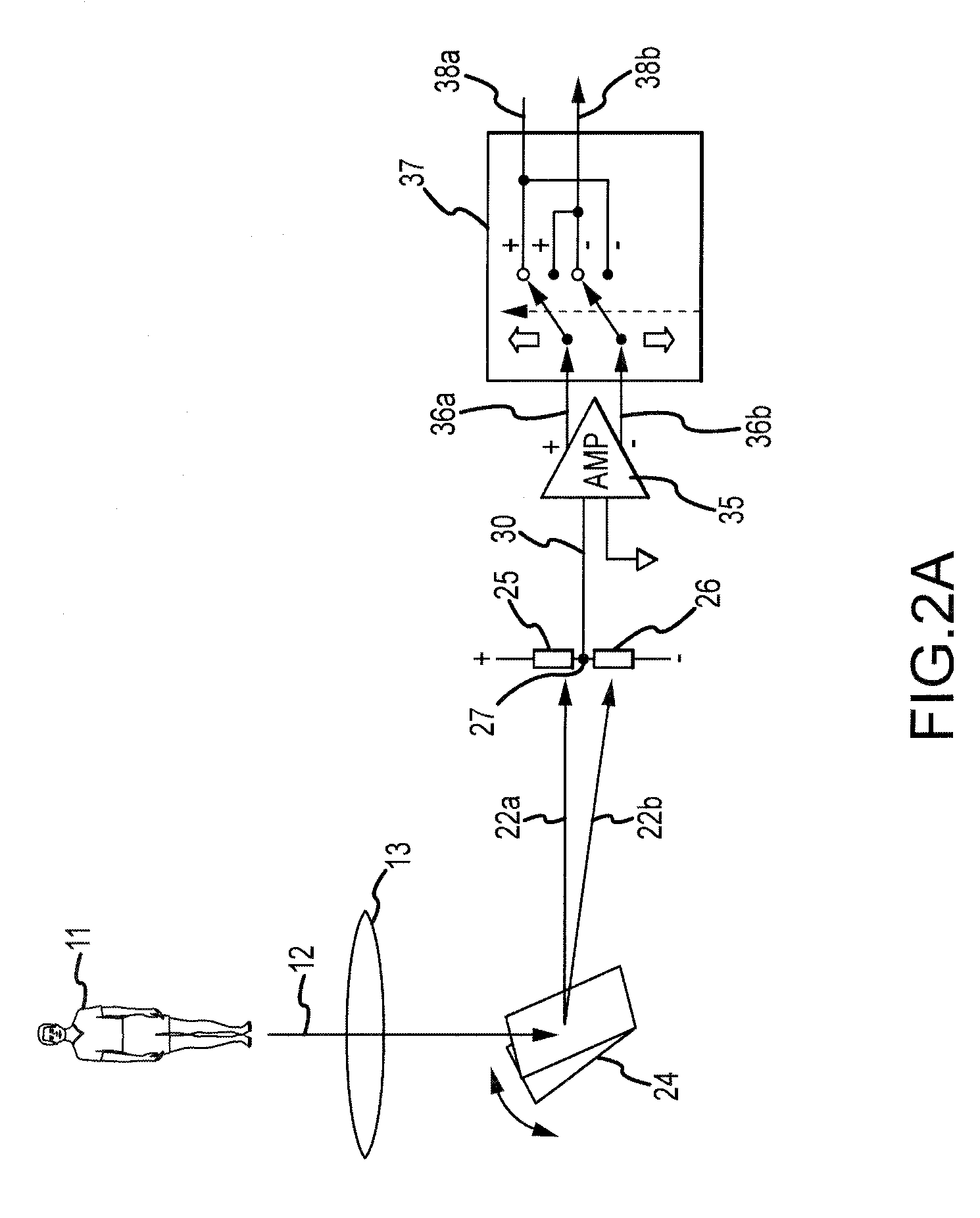
[0011]Following the teaching of the Present Invention, the target input signal (which can be any type of input, such as an optical signal or one of vibration,
magnetic field, sound, heat, pressure, etc.) is split into two components, preferably through a process called “
dither chopping” Each of the two components is then coded, or “tagged,” with a unique marker as the input signal components are converted into an electrical format. The unique encoding technique of the Present Invention maintains
full view of the input scene and does not have scene
blindness problems caused by physical light shutters used in lock-in and
synchronous detection systems. As a consequence, the
noise reduction technology in the detection circuit of embodiments of the Present Invention do not suffer from a 50% loss in input
signal strength occurring in current “
chopper” based systems (e.g., having a physical input
shutter), and, therefore, have up to twice the detection sensitivity. Significantly, the
random noise, containing
white noise and non-
white noise, generated in the system
electronics in embodiments of the Present Invention is suppressed by lowering the non-
white noise with synchronous phase detection and lowering the white noise by enabling reduced bandwidth in operation. In an optical system using the Present Invention, for example, background signals are immediately suppressed at the detector by common mode rejection and the detector system “tagging” each input component with +1 or −1 polarity flags as the signal enters the optical-to-electrical conversion process. The tagged signal components are then synchronized with a second stage of reverse electronic chopping and combined, thereby reestablishing and preserving the original input signal. In this reverse chopping stage, non-white
random noise segments are cancelled and the overall electrical noise effectively attenuated. The simultaneous combination of full-signal non-white
noise suppression by polarity coding, common mode rejection at the sense node and white
noise reduction by
narrow bandwidth has never been taught before. The preservation of the original input signal, while attenuating electronic noise, provides an exceptionally clear, relatively noise-free, visual image.

