Reflective mask, reflective mask blank and method of manufacturing reflective mask

a technology of reflective mask and mask blank, which is applied in the field of reflective mask blank and reflective mask, can solve the problems that the lithography technique using halftone mask is not easily applied as futuristic, and achieve the effects of reducing conductivity, reducing sensitization of resist film, and easy grounding

Active Publication Date: 2013-02-12
HOYA CORP
View PDF11 Cites 6 Cited by
  • Summary
  • Abstract
  • Description
  • Claims
  • Application Information

AI Technical Summary

Benefits of technology

[0036]A reflective mask according to this invention includes a multilayer reflective film, on a substrate, having a structure in which high refractive index layers and low refractive index layers are alternately laminated, and an absorbing film stacked on the multilayer reflective film and adapted to absorb EUV exposure light. The absorbing film is a phase shift film that allows the EUV exposure light having passed therethrough and reflected by the multilayer reflective film to have a predetermined phase difference with respect to the EUV exposure light directly incident on and reflected by the multilayer reflective film. A plurality of the layers or all the layers of the multilayer reflective film in a blind area are removed from its upper layer.
[0037]According to this structure, since all the layers of the multilayer reflective film in the blind area are removed or a plurality of the layers thereof are removed to a degree such that the multilayer reflective film does not substantially have a function as a multilayer reflective film, even if the EUV exposure light leaks to the blind area, it is hardly reflected. Thus, there is an effect that even if transfer patterns are transferred on a resist film of a transfer target with almost no gap therebetween using this reflective mask such that the blind area to which the EUV exposure light leaks overlaps the adjacent transfer pattern, it is possible to suppress sensitization of the resist film of the transfer target at a portion that should not primarily be sensitized, i.e. at an overlapping portion between the blind area and an absorbing film remaining portion of the adjacent transfer pattern.
[0038]In the invention of a reflective mask blank of this invention having a conductive film, there is the following effect. In the case where a reflective mask, in which all or a plurality of layers of a multilayer reflective film in a blind area are removed, is manufactured using a related reflective mask blank, it may be difficult to ensure grounding of the multilayer reflective film in a transfer area which is most apt to be electrostatically charged, due to a decrease in conductivity at the removed portion. Since the reflective mask blank of this invention has the conductive film between a substrate and a multilayer reflective film, there is an effect that the multilayer reflective film in a transfer area can be easily grounded by grounding the conductive film.

Problems solved by technology

However, even with the ArF excimer laser, in terms of additional problems in exposure apparatus and resist, the lithography technique using the halftone mask is not easily applied as a futuristic lithography technique for manufacturing a device with a line width of 50 nm or less.

Method used


Image

  • Reflective mask, reflective mask blank and method of manufacturing reflective mask
  • Reflective mask, reflective mask blank and method of manufacturing reflective mask
  • Reflective mask, reflective mask blank and method of manufacturing reflective mask

Examples


example 1

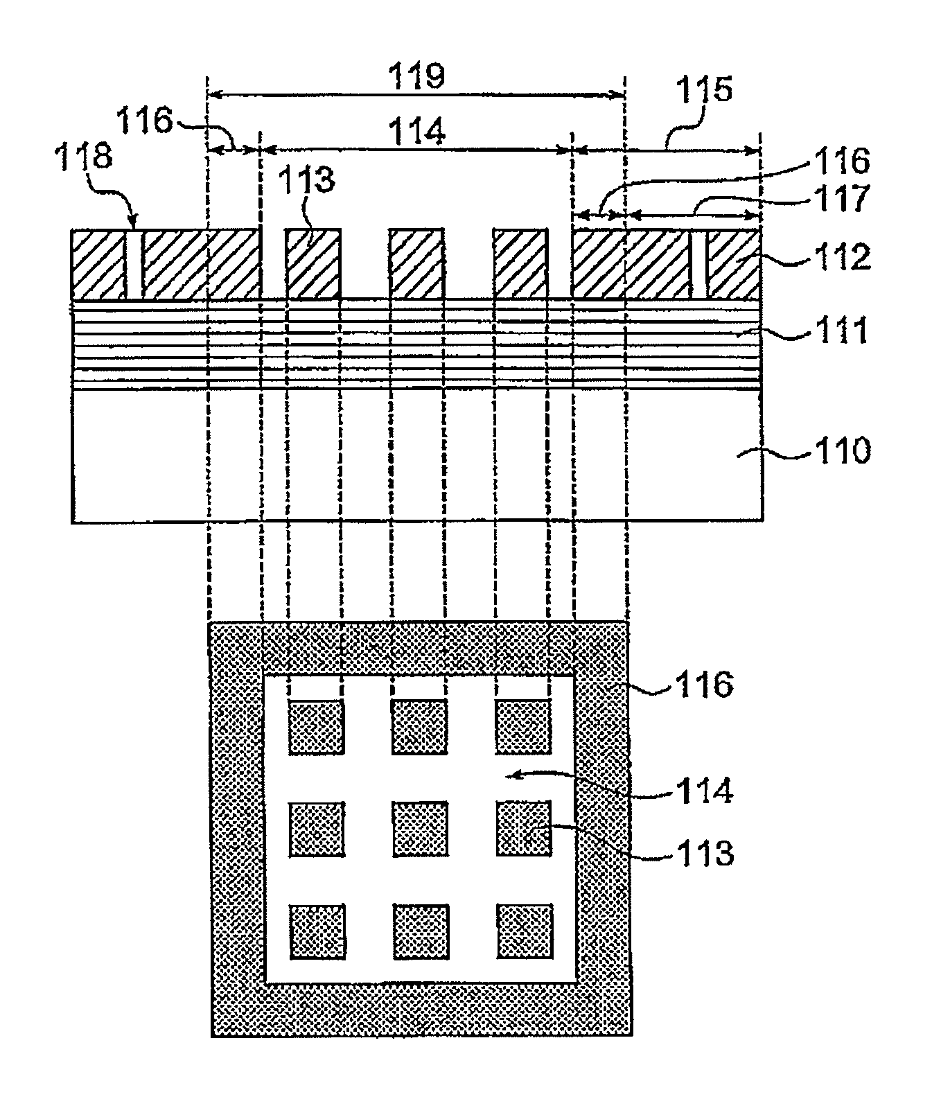
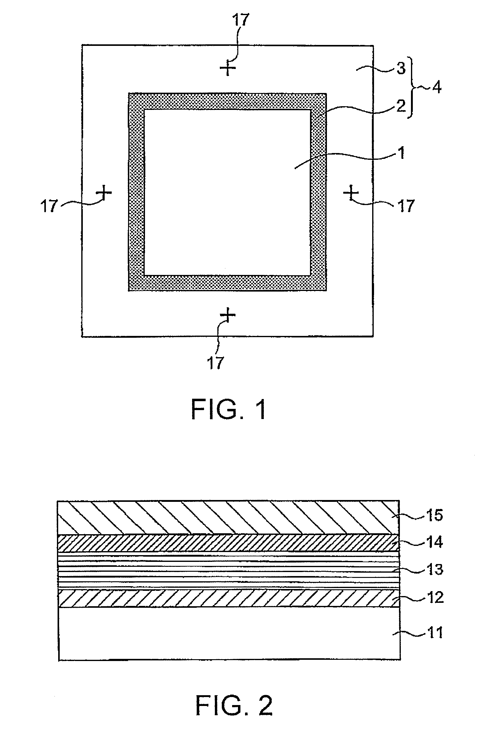
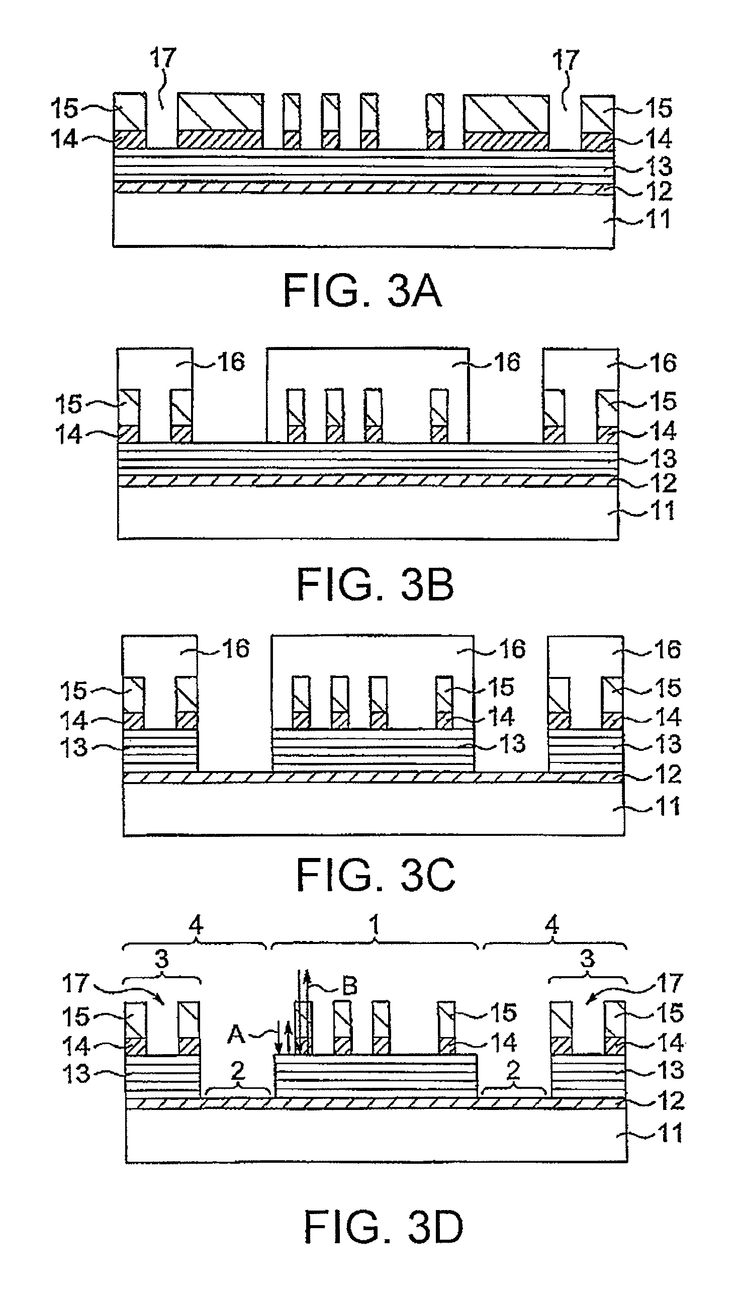
[0085]First, as a substrate, there was prepared a low-expansion SiO2—TiO2-based glass substrate having an external shape of 152 mm square with a thickness of 6.3 mm. Then, chromium nitride (CrN: N=10 at %) was coated on the substrate by DC magnetron sputtering, thereby forming a conductive film having a thickness of 5 nm. Then, Mo and Si suitable as reflective films in the region of an exposure wavelength 13 to 14 nm being a wavelength of EUV light were coated on the conductive film by ion beam sputtering, thereby forming a multilayer reflective film having a total thickness of 284 nm (Mo:2.8 nm, Si:4.2 nm, given that this forms one cycle, Si and Mo films were laminated by 40 cycles and, finally, a Si film was formed to 4 nm thick).

[0086]Then, chromium nitride (CrN: N=10 at %) was coated on the multilayer reflective film by DC magnetron sputtering, thereby forming a buffer film having a thickness of 10 nm. Then, TaN was coated on the buffer film by DC magnetron sputtering, thereby f...

example 2

[0093]First, as a substrate, there was prepared a low-expansion SiO2—TiO2-based glass substrate having an external shape of 152 mm square with a thickness of 6.3 mm. Then, chromium nitride (CrN: N=10 at %) was coated on the substrate by DC magnetron sputtering, thereby forming a conductive film having a thickness of 5 nm. Then, Mo and Si suitable as reflective films in the region of an exposure wavelength 13 to 14 nm being a wavelength of EUV light were coated on the conductive film by ion beam sputtering, thereby forming a multilayer reflective film having a total thickness of 284 nm (Mo:2.8 nm, Si:4.2 nm, given that this forms one cycle, Si and Mo films were laminated by 40 cycles and, finally, a Si film was formed to 4 nm thick).

[0094]Then, chromium nitride (CrN: N=10 at %) was coated on the multilayer reflective film by DC magnetron sputtering, thereby forming a buffer film having a thickness of 10 nm. Then, TaBN was coated on the buffer film by DC magnetron sputtering, thereby ...

example 3

[0101]First, as a substrate, there was prepared a low-expansion SiO2—TiO2-based glass substrate having an external shape of 152 mm square with a thickness of 6.3 mm. Then, Mo and Si suitable as reflective films in the region of an exposure wavelength 13 to 14 nm being a wavelength of EUV light were coated on the substrate by ion beam sputtering, thereby forming a multilayer reflective film having a total thickness of 284 nm (Mo:2.8 nm, Si:4.2 nm, given that this forms one cycle, Si and Mo films were laminated by 40 cycles and, finally, a Si film was formed to 4 nm thick).

[0102]Then, chromium nitride (CrN: N=10 at %) was coated on the multilayer reflective film by DC magnetron sputtering, thereby forming a buffer film having a thickness of 10 nm. Then, TaN was coated on the buffer film by DC magnetron sputtering, thereby forming a semitransmissive film having a thickness of 28 nm. In this event, the film formation was carried out using a tantalum target and using an Ar gas added with...


PUM

PropertyMeasurementUnit
wavelengthaaaaaaaaaa
transmittanceaaaaaaaaaa
wavelengthaaaaaaaaaa

Abstract

A reflective mask of this invention includes a multilayer reflective film (13), on a substrate (11), having a structure in which high refractive index layers and low refractive index layers are alternately laminated, and an absorbing film (15) stacked on the multilayer reflective film (13) and adapted to absorb EUV exposure light. The absorbing film (15) is a phase shift film that allows the EUV exposure light having passed therethrough and reflected by the multilayer reflective film to have a predetermined phase difference with respect to the EUV exposure light directly incident on and reflected by the multilayer reflective film. A plurality of the layers or all the layers of the multilayer reflective film (13) in a blind area are removed from its upper layer.

Description

TECHNICAL FIELD[0001]This invention relates to a reflective mask blank and a reflective mask. More specifically, this invention relates to a reflective mask suitable as a reflective mask for use in a lithography method using exposure light in a short wavelength region such as extreme ultraviolet light and to a reflective mask blank for such a reflective mask.BACKGROUND ART[0002]In recent years, with higher integration of semiconductor devices, fine patterns exceeding the transfer limit of a photolithography method using the conventional ultraviolet light have been required in the semiconductor industry. In order to enable transfer of such fine patterns, the EUV lithography being an exposure technique using extreme ultraviolet light (hereinafter referred to as EUV light) with a shorter wavelength is expected to be promising. The EUV light represents light in a wavelength band of the soft X-ray region or the vacuum ultraviolet region and, specifically, light having a wavelength of abo...

Claims


Application Information

Patent Timeline
Patent Type & Authority Patents(United States)
IPC IPC(8): G03F1/24G03F1/26
CPCB82Y10/00B82Y40/00G03F1/24G03F1/26H01L21/0275
Inventor SHOKI, TSUTOMU
Owner HOYA CORP
Why Eureka
Try Eureka