Reflective mask blank, reflective mask, and method of manufacturing the same
a technology of reflective mask and mask blank, which is applied in the field of reflective mask blank and reflective mask, can solve the problems of not being able to apply it as a futuristic lithography technique, and achieve the effect of suppressing the sensitization of the resist layer
- Summary
- Abstract
- Description
- Claims
- Application Information
AI Technical Summary
Benefits of technology
Problems solved by technology
Method used
Image
Examples
example 1
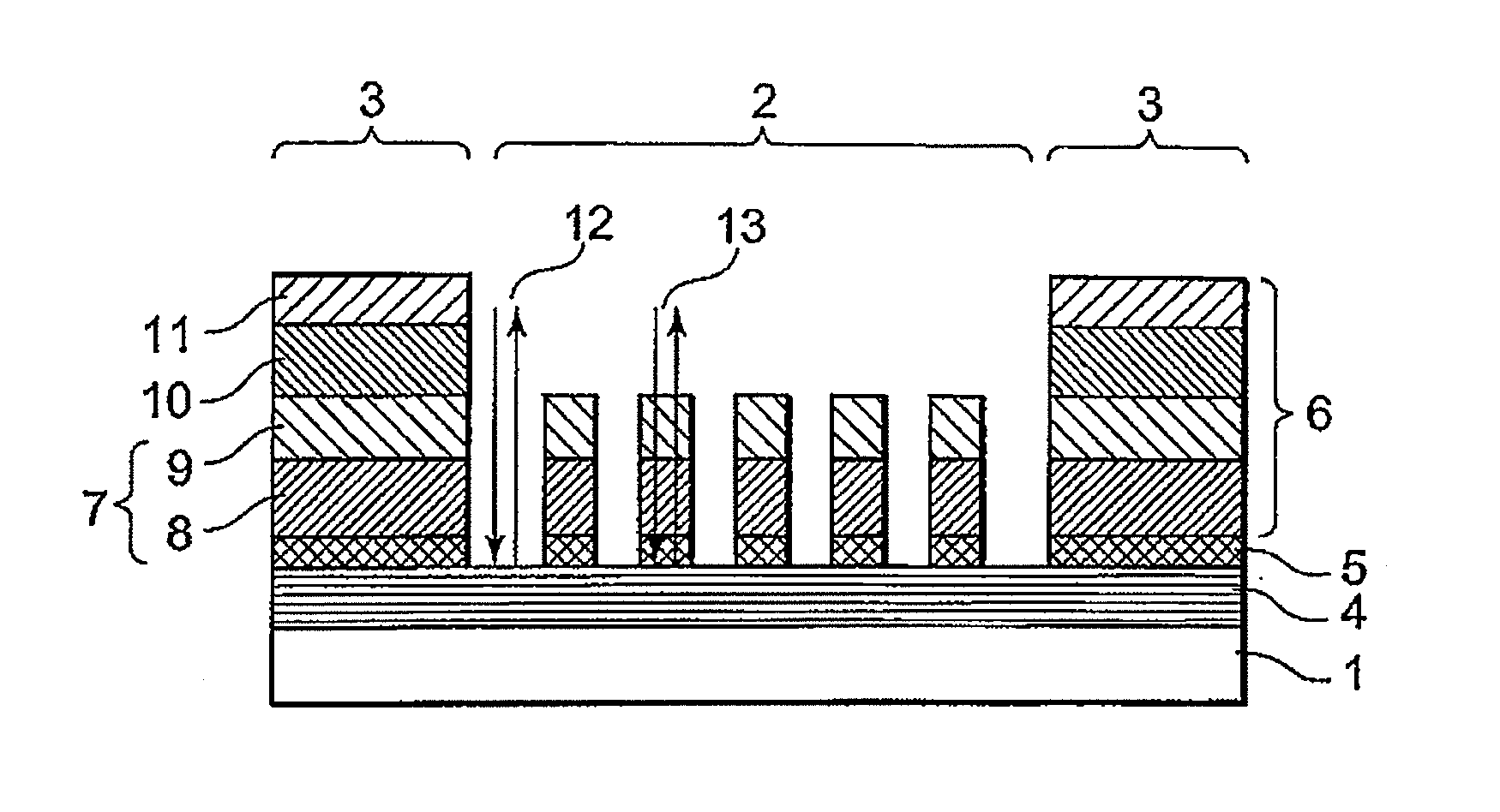
[0065]Hereinbelow, the embodiment of this invention will be described in further detail with reference to Examples. First, a manufacturing method of a reflective mask in this Example will be described with reference to the drawings.
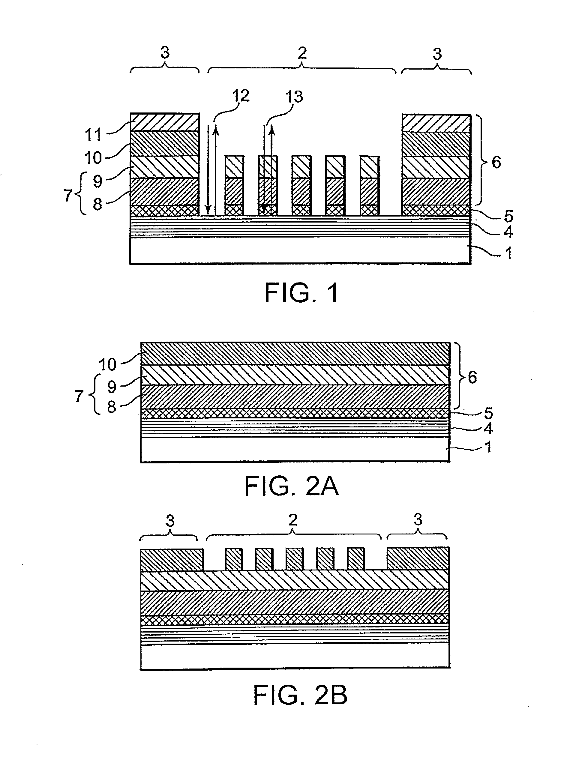
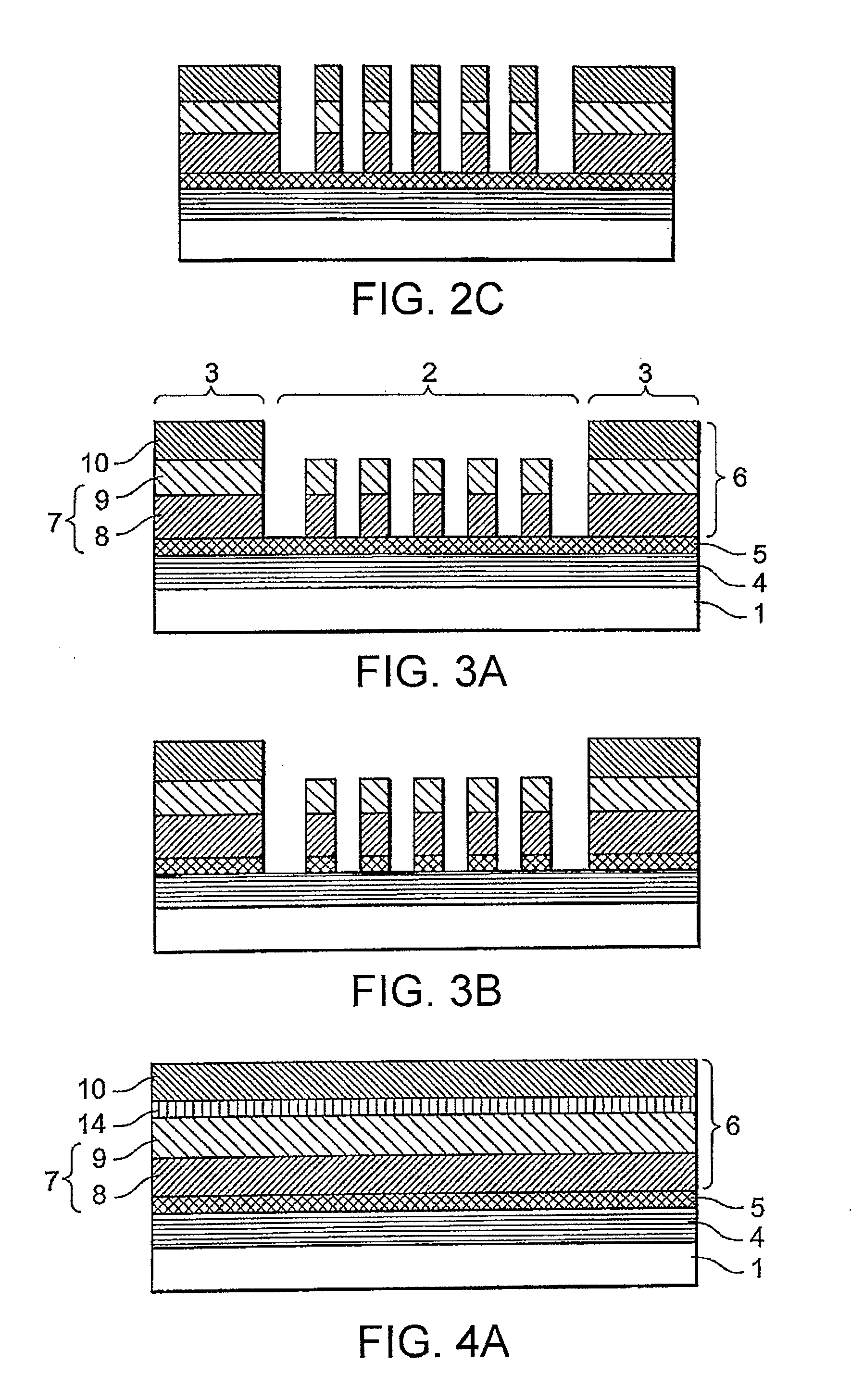
[0066]FIGS. 2A to 2C and FIGS. 3A and 3B are diagrams showing cross-sectional structures of manufacturing processes of the reflective mask according to this Example.
[0067]As shown in FIG. 2A, a reflective mask blank was manufactured. First, as a substrate 1, there was prepared a low-expansion SiO2—TiO2-based glass substrate having an external shape of 152 mm square with a thickness of 6.3 mm.
[0068]Then, an alternately laminated film of Mo and Si suitable as reflective films in the region of a wavelength 13 to 14 nm being a wavelength of EUV light was formed as a multilayer reflective film 4 on the substrate 1. The film formation was carried out using an ion beam sputtering apparatus. A Si target was first used to form a Si film to 4.2 nm thick, then a Mo ...
example 2
[0081]Hereinbelow, as Example 2, there is shown a case where, in Example 1, the semitransmissive layer 8 was, instead of the TaN film, a film (TaBN film) composed mainly of Ta and containing B and N, the antireflection layer 9 was, instead of the TaO film, a film (TaBO film) composed mainly of Ta and containing B and O, and the absorber layer 10 was, instead of the TaN film, a film (TaBN film) composed mainly of Ta and containing B and N. The other structure was the same as in Example 1.
[0082]The TaBN film forming the semitransmissive film 8 was formed on a buffer film 5 by the DC magnetron sputtering method using a sintered body target containing tantalum and boron and using an Ar gas added with 40% nitrogen. The film thickness was set to 30 nm as a thickness capable of semitransmitting EUV exposure light. The composition ratio of the formed TaBN film was such that Ta:B:N=60:10:30.
[0083]The TaBO film forming the antireflection layer 9 was formed to 14 nm thick on the semitransmissi...
example 3
[0088]Hereinbelow, as Example 3, there is shown a case where, in Example 1, the semitransmissive layer 8 was, instead of the TaN film, a film (TaB film) composed mainly of Ta and containing B, the antireflection layer 9 was, instead of the TaO film, a film (TaBO film) composed mainly of Ta and containing B and O, and the absorber layer 10 was, instead of the TaN film, a film (TaB film) composed mainly of Ta and containing B. The other structure was the same as in Example 1.
[0089]The TaB film forming the semitransmissive film 8 was formed on a buffer film 5 by the DC magnetron sputtering method using a sintered body target containing tantalum and boron and using an Ar gas. The film thickness was set to 28 nm as a thickness capable of semitransmitting EUV exposure light. The composition ratio of the formed TaBN film was such that Ta:B=80:20.
[0090]The TaBO film forming the antireflection layer 9 was formed to 14 nm thick on the semitransmissive film 8 by the DC magnetron sputtering met...
PUM
| Property | Measurement | Unit |
|---|---|---|
| wavelength | aaaaa | aaaaa |
| transmittance | aaaaa | aaaaa |
| wavelength | aaaaa | aaaaa |
Abstract
Description
Claims
Application Information


