Thin film transistor substrate and flat panel display apparatus

a thin film transistor and substrate technology, applied in transistors, electrical devices, semiconductor devices, etc., can solve the problems of degrading the image quality characteristics of the flat panel display apparatus, degrading the electrical characteristics of each of the thin film transistors, etc., to achieve uniform display characteristics and easy provision of electrical characteristics. uniform

Inactive Publication Date: 2013-03-19
SAMSUNG DISPLAY CO LTD
View PDF46 Cites 0 Cited by
  • Summary
  • Abstract
  • Description
  • Claims
  • Application Information

AI Technical Summary

Benefits of technology

[0009]The present invention provides a thin film transistor substrate and a flat panel display apparatus which easily provide uniform electrical characteristics and uniform display characteristics.

Problems solved by technology

The protrusions interrupt the flow of current, thereby degrading the electrical characteristics of each of the thin film transistors.
Also, the protrusions irregularly distributed on the channel region degrade the uniform electrical characteristics of the thin film transistor substrate, thereby degrading the image quality characteristics of the flat panel display apparatus.

Method used


Image

  • Thin film transistor substrate and flat panel display apparatus
  • Thin film transistor substrate and flat panel display apparatus
  • Thin film transistor substrate and flat panel display apparatus

Examples


Embodiment Construction

[0018]The present invention will now be described more fully with reference to the accompanying drawings, in which exemplary embodiments of the invention are shown.

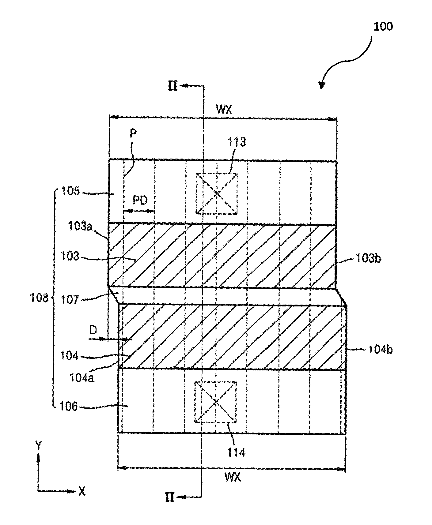
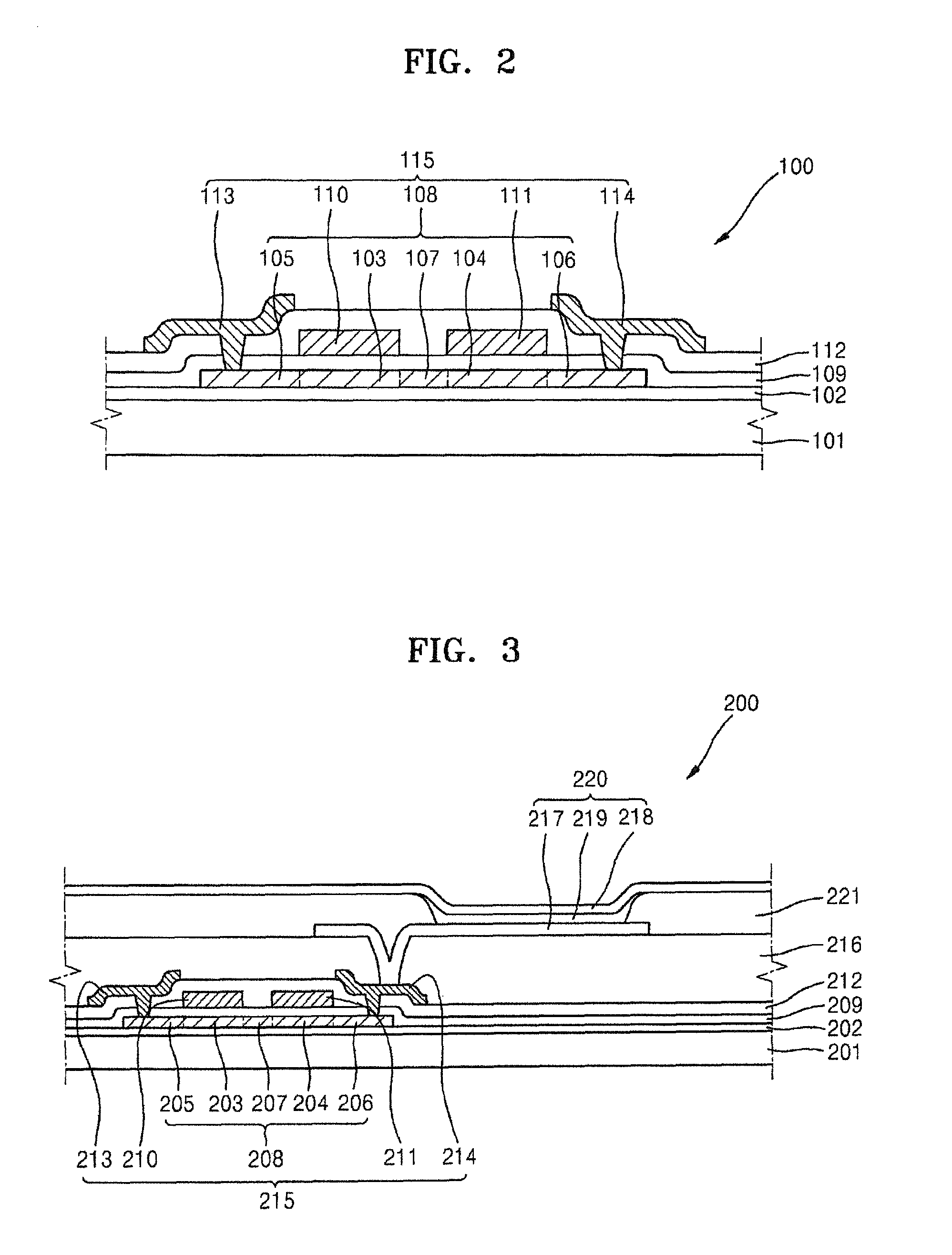
[0019]Turning now to FIGS. 1 and 2, FIG. 1 is a plan view of a thin film transistor substrate 100 according to an embodiment of the present invention and FIG. 2 is a cross-sectional view taken along line II-II of FIG. 1. Referring to FIGS. 1 and 2, the thin film transistor substrate 100 includes a plurality of thin film transistors arranged on a substrate 101, however for convenience of explanation, only one thin film transistor 115 is illustrated in FIGS. 1 and 2.

[0020]Specifically, the substrate 101 may be a transparent glass material including SiO2 as a main component, however the present embodiment is not limited thereto, as the substrate 101 may instead be made out of a transparent plastic material. If the substrate 101 is made out of a transparent plastic material, the transparent plastic material may be an organic ...


PUM


Abstract

A thin film transistor substrate including a plurality of thin film transistors, and a flat panel display apparatus. Each of the plurality of thin film transistors includes an active layer comprising a first channel region having a first plurality of protrusion lines arranged therein and a second channel region and having a second plurality of protrusion lines arranged therein, a source electrode and a drain electrode electrically connected to the active layer and a gate electrode insulated from the active layer, wherein the first and second plurality of protrusion lines extend in a first direction, wherein a edges of the first channel region that extend in the first direction and are offset sideways by a distance in a second direction that is orthogonal to the first direction from corresponding edges of the second channel region that extend in the first direction.

Description

CLAIM OF PRIORITY[0001]This application makes reference to, incorporates the same herein, and claims all benefits accruing under 35 U.S.C. §119 from an application for a THIN FILM TRANSISTOR SUBSTRATE AND FLAT PANEL DISPLAY APPARATUS earlier filed in the Korean Intellectual Property Office on 26 Aug. 2010 and there duly assigned Serial No. 10-2010-0083061.BACKGROUND OF THE INVENTION[0002]1. Field of the Invention[0003]The present invention relates to a thin film transistor substrate and a flat panel display apparatus that has uniform electrical characteristics and uniform display characteristics.[0004]2. Description of the Related Art[0005]Recently, many existing display apparatuses are replaced by flat panel display apparatuses that are portable and thin. Of among flat panel display apparatuses, liquid crystal display apparatuses and organic light-emitting display apparatuses appeal most to people because of their excellent image quality and their portability.[0006]Meanwhile, such ...

Claims


Application Information

Patent Timeline
Patent Type & Authority Patents(United States)
IPC IPC(8): H01L29/786
CPCH01L27/1285H01L27/1296H01L29/04H01L29/78645H01L29/78696H01L29/34
Inventor SHIN, KWANG-SUB
Owner SAMSUNG DISPLAY CO LTD
Why Eureka
Try Eureka