Designing an optimal wiring topology for electromigration avoidance

a topology and wire technology, applied in the direction of error detection/correction, program control, instruments, etc., can solve the problems of void and hillock on the wire, affecting the layout of the circuit, and consuming enormous routing resources

Inactive Publication Date: 2013-03-19
NAT CHIAO TUNG UNIV
View PDF7 Cites 2 Cited by
  • Summary
  • Abstract
  • Description
  • Claims
  • Application Information

AI Technical Summary

Problems solved by technology

Therefore, as the long term usage of the chip or the current density of the wire exceeding the process limitation, a mass of atoms inside of the metal wire are forced to migrate along the direction of the current, and the gradual transport eventually causes the void and the hillock formed on the wire.
For example, the failure of the chip is triggered when the hillock of the wire contacting with the neighbor.
However, the conventional EM fixing is applied at post-layout, which may consume tremendous routing resources and induce a large amount of layout change.
However, the tree edge is able be provided only from DT edges; thus, if the solution must include a non-DT edge, the wiring topology fails.
Consequently, how to find the optimal wiring topology to avoid electromigration and to save the routing resource is an important issue.

Method used


Image

  • Designing an optimal wiring topology for electromigration avoidance
  • Designing an optimal wiring topology for electromigration avoidance
  • Designing an optimal wiring topology for electromigration avoidance

Examples


Embodiment Construction

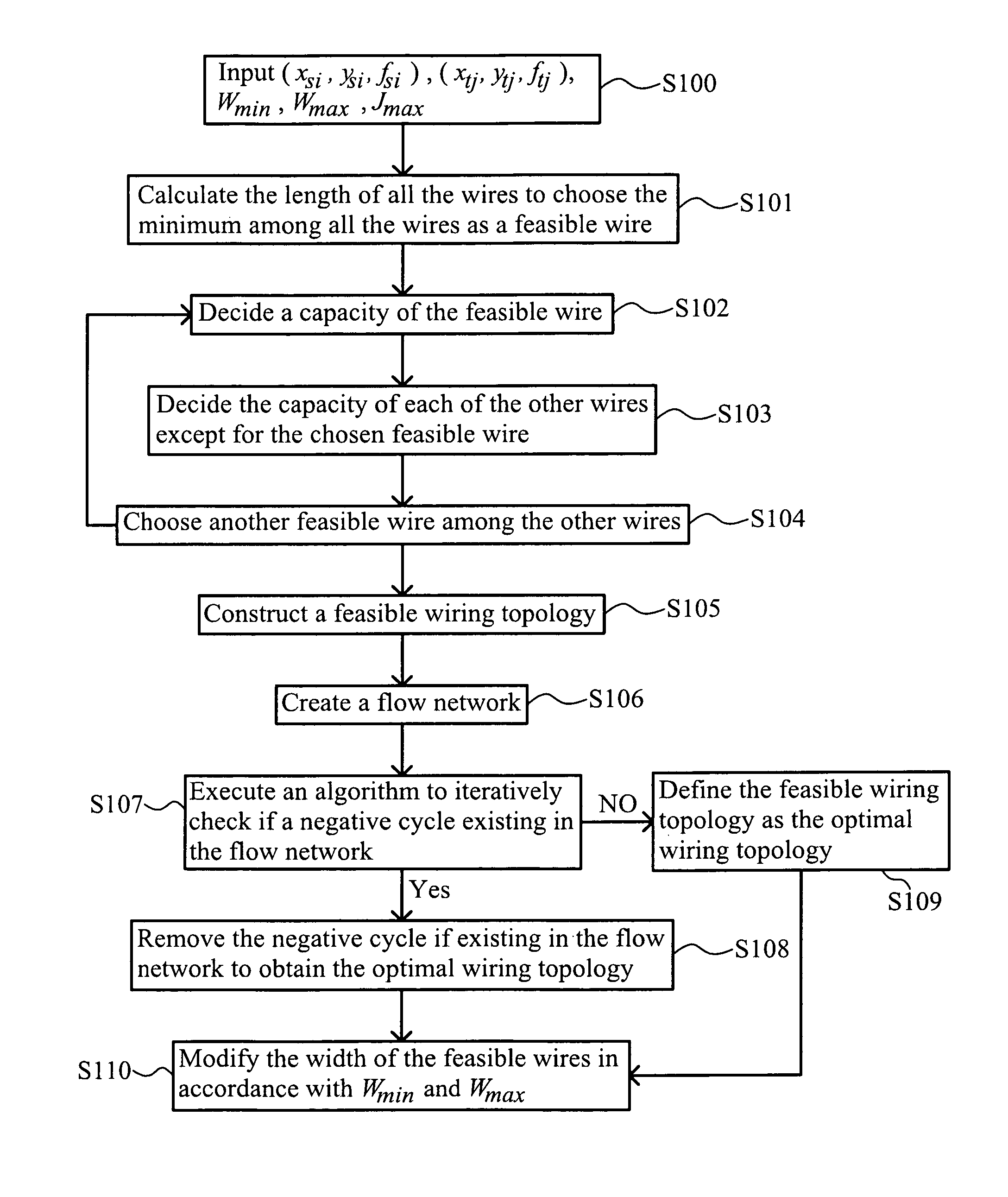
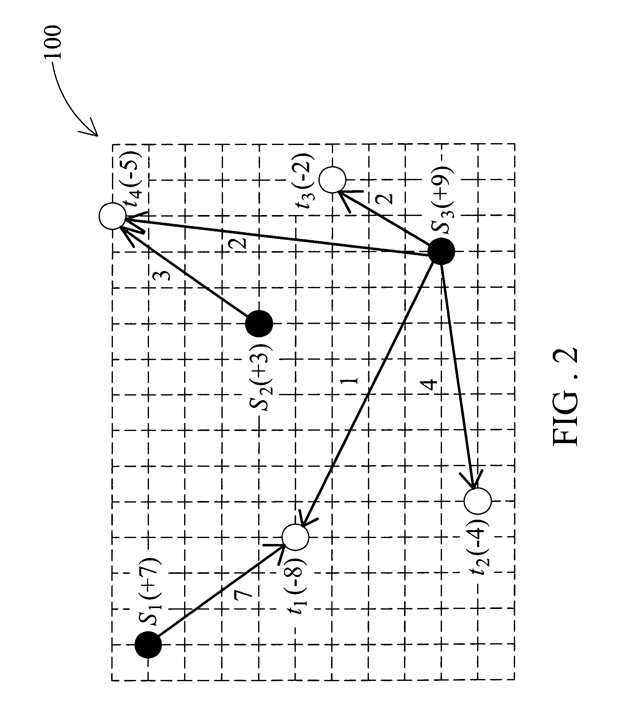
[0032]In the following detailed description of the preferred embodiments, reference is made to the accompanying drawings which form a part hereof, and in which is shown by way of illustration specific embodiments in which the invention may be practiced. In this regard, directional terminology, such as “top,”“bottom,”“front,”“back,” etc., is used with reference to the orientation of the Figure(s) being described. The components of the present invention can be positioned in a number of different orientations. As such, the directional terminology is used for purposes of illustration and is in no way limiting. On the other hand, the drawings are only schematic and the sizes of components may be exaggerated for clarity. It is to be understood that other embodiments may be utilized and structural changes may be made without departing from the scope of the present invention. Also, it is to be understood that the phraseology and terminology used herein are for the purpose of description and...


PUM


Abstract

A method for designing an optimal wiring topology for electromigration avoidance is disclosed. The wiring topology includes multiple sources, multiple sinks and multiple wires. The method includes the following steps: A feasible wire, a wire of the shortest length connecting each pair of source and sink, is calculated, and the capacity of each feasible wire is decided. An initial feasible topology is found. A flow network is created based on the initial topology. Negative cycles are iteratively checked and removed until no more negative cycles.

Description

BACKGROUND OF THE INVENTION[0001](1) Field of the Invention[0002]The invention relates to a method for designing wiring topology and a fabrication method of integrated circuits including said method, and especially relates to a method for designing optimal wiring topology applied for electromigration avoidance in an integrated circuit.[0003](2) Description of the Prior Art[0004]For the shrinking feature size and multiple functions of the chip, the components and the designed wires thereof disposed on the chip are more complex, so the size of the wires should be shrunk. Therefore, as the long term usage of the chip or the current density of the wire exceeding the process limitation, a mass of atoms inside of the metal wire are forced to migrate along the direction of the current, and the gradual transport eventually causes the void and the hillock formed on the wire. Said phenomenon is referred to as electromigration (EM), and the electromigration causes a permanent failure, such as ...

Claims


Application Information

Patent Timeline
Patent Type & Authority Patents(United States)
IPC IPC(8): G06F17/50G06F9/455G06F11/22
CPCG06F17/5077G06F2217/82G06F30/394G06F2119/10
Inventor JIANG, HUI-RUCHANG, HUA-YUCHANG, CHIH-LONG
Owner NAT CHIAO TUNG UNIV
Why Eureka
Try Eureka