Unlock instant, AI-driven research and patent intelligence for your innovation.

Data transmission device

a data transmission device and semiconductor memory technology, applied in the direction of information storage, static storage, digital storage, etc., can solve the problems of inefficient programmable stress test time, slow clock signal inputted from programmable stress test equipment, and slow clock signal input from high speed clock signal

Active Publication Date: 2013-06-04
SK HYNIX INC
View PDF9 Cites 2 Cited by
  • Summary
  • Abstract
  • Description
  • Claims
  • Application Information

AI Technical Summary

Problems solved by technology

However, a clock signal inputted from a programmable stress test equipment is slower than a high speed clock signal operable in the semiconductor memory apparatus.
First, when a fail in the cell has occurred during the data input / output operation, it is necessary to avoid a situation in which it may not be possible to determine whether the reason for the fail is caused by the lack of a margin for a high speed operation or the abnormal operation of the cell, that is, it is necessary to ensure the reliability of the programmable stress test.
Second, since the semiconductor memory apparatus operating at a higher speed is tested using a traditional programmable stress test equipment, the high speed clock signal operable in the semiconductor memory apparatus may be faster than a clock signal inputted from the programmable stress test equipment.
Since the period of the clock signal used for the programmable stress test may be longer than that of the high speed clock signal operable in the semiconductor memory apparatus, and an input command may not be inputted in four periods of a clock according to the 8-bit pre-fetch scheme and the DDR scheme as described above, the programmable stress test time is inefficiently increased.
Such a problem becomes severer as the semiconductor memory apparatus is highly integrated and operates at a high speed.
Since the increase in the test time may cause an increase in the production time of the semiconductor memory apparatus, the semiconductor memory apparatus has disadvantages in terms of the production cost and manufacturing efficiency.

Method used


Image

  • Data transmission device
  • Data transmission device
  • Data transmission device

Examples


Embodiment Construction

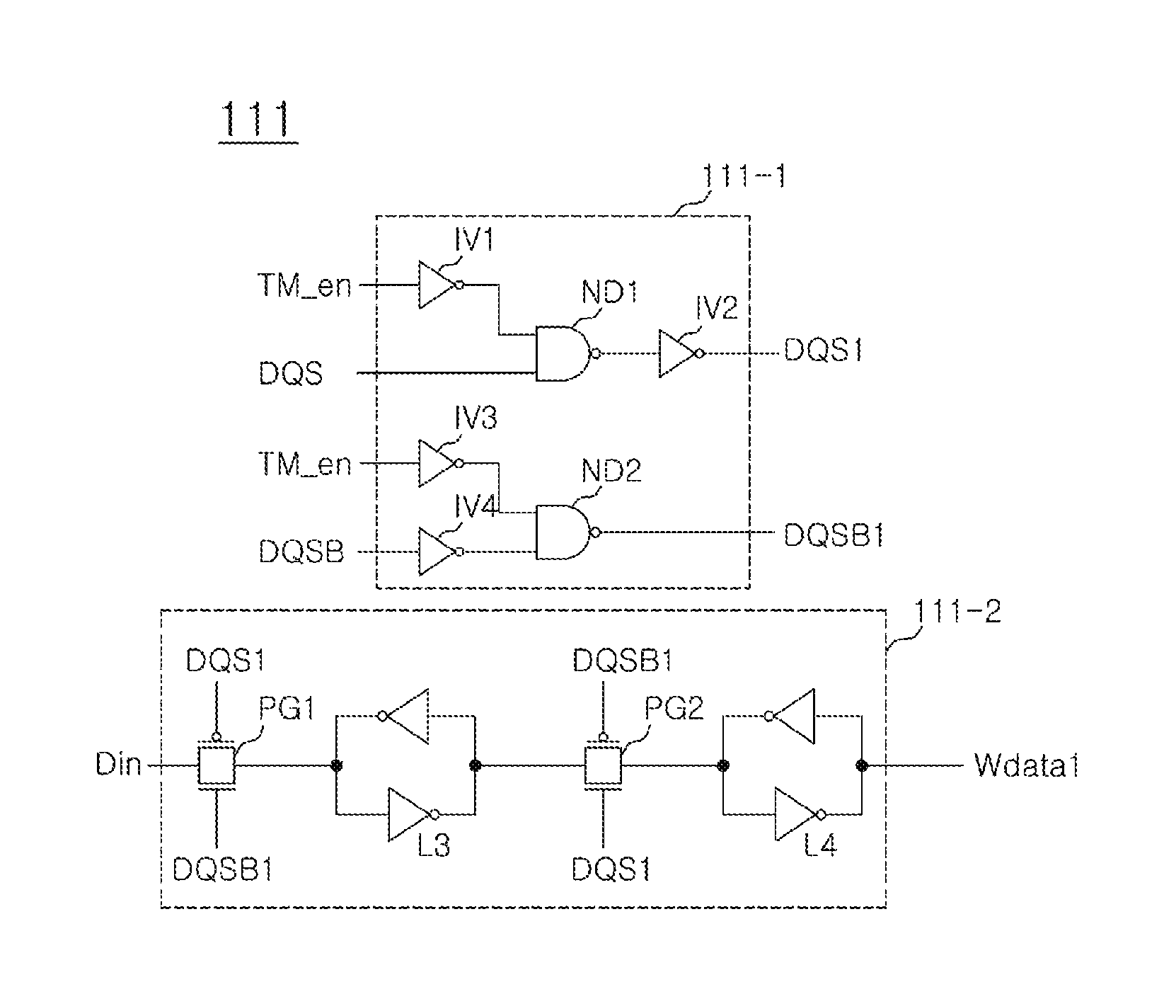
[0027]A data transmission device according to one embodiment may reduce input time of a programmable stress test by allowing data which is to be inputted at the time of the programmable stress test, to be received using a test mode signal, instead of receiving the data through data pads. Since the programmable stress test is used to check whether a cell is capable of performing normal input / output operations, it may be possible to test the capacity of a cell to perform normal data input / output operations even if the data is not necessarily received from the data pads. In this regard, the data transmission device according to one embodiment includes elements configured to latch normal data and elements configured to output predetermined test data, and may directly apply the predetermined test data to input / output lines, without waiting for data input from the data pads at the start of the programmable stress test.

[0028]FIG. 4 is a schematic block diagram of the data transmission devi...


PUM


Abstract

A data transmission device in a semiconductor memory apparatus receives input data via a local data input / output line and output s the input data on a plurality of global data input / output lines. The data transmission device includes a write data generation block configured to receive the input data and test data and output one of input data and test data as write data in response to an activation of a test enable signal, and a loading block configured to apply the write data to one of the plurality of global data input / output lines in response to an enable signal.

Description

CROSS-REFERENCES TO RELATED APPLICATION[0001]The present application claims priority under 35 U.S.C. §119(a) to Korean Application No. 10-2010-0051292, filed on May 31, 2010, in the Korean Intellectual Property Office, which is incorporated herein by reference in its entirety as if set forth in full.BACKGROUND[0002]1. Technical Field[0003]The present invention relates to a semiconductor memory apparatus, and more particularly, to a semiconductor memory apparatus including a data transmission device.[0004]2. Related Art[0005]Data input operations in a synchronous semiconductor memory apparatus are typically performed in synchronization with an internal clock signal which is generated based on an external clock signal. The synchronous semiconductor memory apparatus uses a pre-fetch scheme and may input multi-bit data in response to one-time input command. The pre-fetch scheme is a data input method by which serial multi-bit data sequentially inputted to each data pad in response to on...

Claims


Application Information

Patent Timeline
Patent Type & Authority Patents(United States)
IPC IPC(8): G11C7/00
CPCG11C29/1201G11C29/48
Inventor KU, YOUNG JUN
Owner SK HYNIX INC