Method for manufacturing solid-state image pickup device

a solid-state image and pickup device technology, applied in the direction of semiconductor devices, basic electric elements, electrical appliances, etc., can solve the problems of polysilicon film undetected in narrow spaces, degradation of image quality, charge leakage, etc., and achieve the effect of improving yield

Active Publication Date: 2013-10-08
CANON KK
View PDF8 Cites 3 Cited by
  • Summary
  • Abstract
  • Description
  • Claims
  • Application Information

AI Technical Summary

Benefits of technology

[0010]One disclosed aspect of the embodiments provides a manufacturing method which improves yields while maintaining the optical properties of a solid-state image pickup device having a light-shielding film.

Problems solved by technology

If charges generated in parts other than the photoelectric conversion element flow into the charge holding part during this period, the charges may become a noise signal, and consequently degrade the image quality.
In the case where a polysilicon film is patterned, the polysilicon film may undesirably remain in narrow spaces between the gate electrodes of transistors arranged in the peripheral circuit portion.
This remaining polysilicon film causes charge leakage and reduces yields.
However, this method degrades the optical properties of the solid-state image pickup device because the distance between each photoelectric conversion element and a corresponding microlens disposed on the topmost surface increases.
Such a drawback also occurs in another configuration described in Japanese Patent Laid-Open No. 2007-115803 in which the light-shielding film is formed of a non-polysilicon film, e.g., a metal film of tungsten, etc.
In addition, the same drawback may occur when a light-shielding film having a slit is formed in a solid-state image pickup device disclosed in Japanese Patent Laid-Open No. 2009-105358.

Method used


Image

  • Method for manufacturing solid-state image pickup device
  • Method for manufacturing solid-state image pickup device
  • Method for manufacturing solid-state image pickup device

Examples


first embodiment

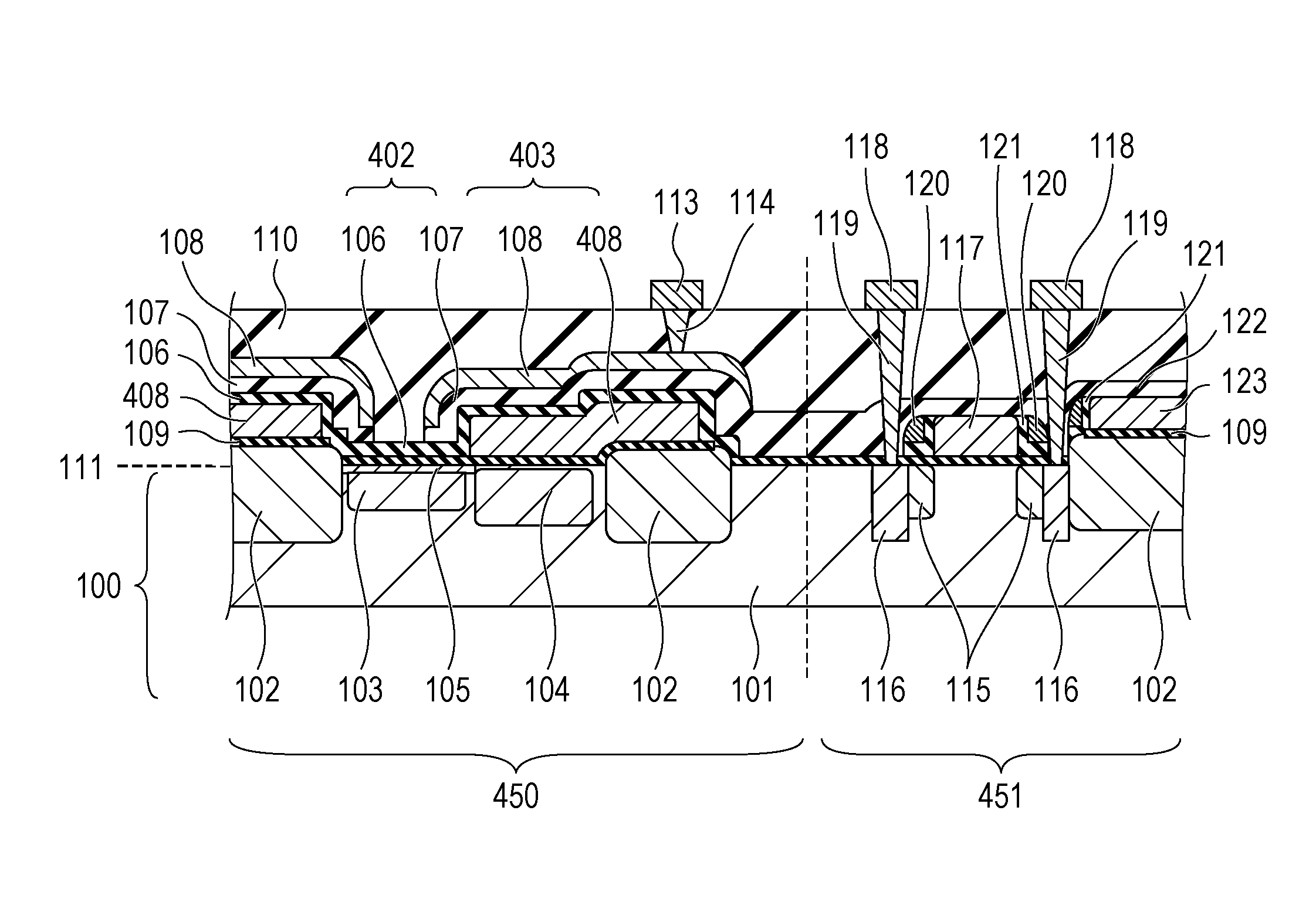
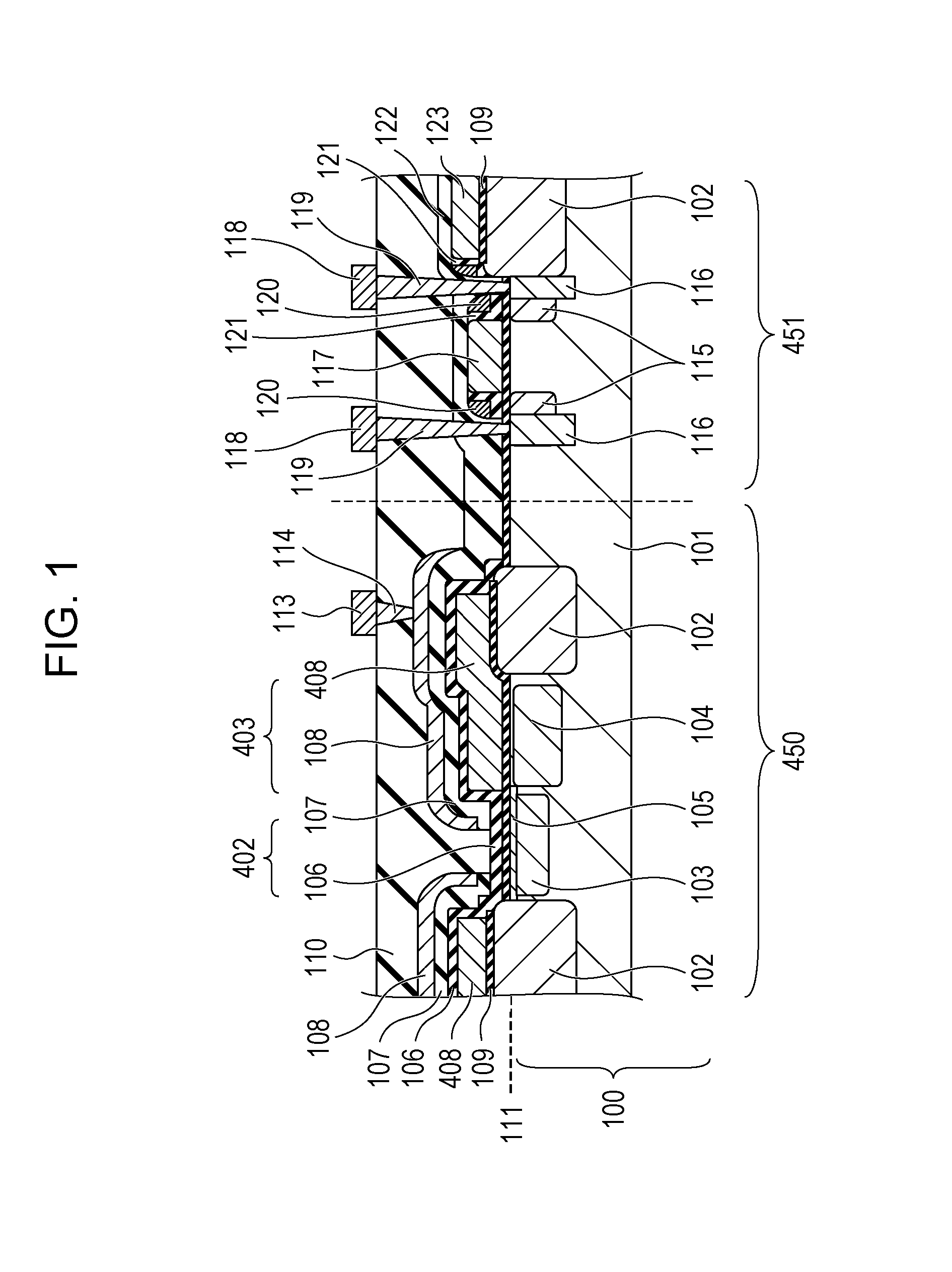
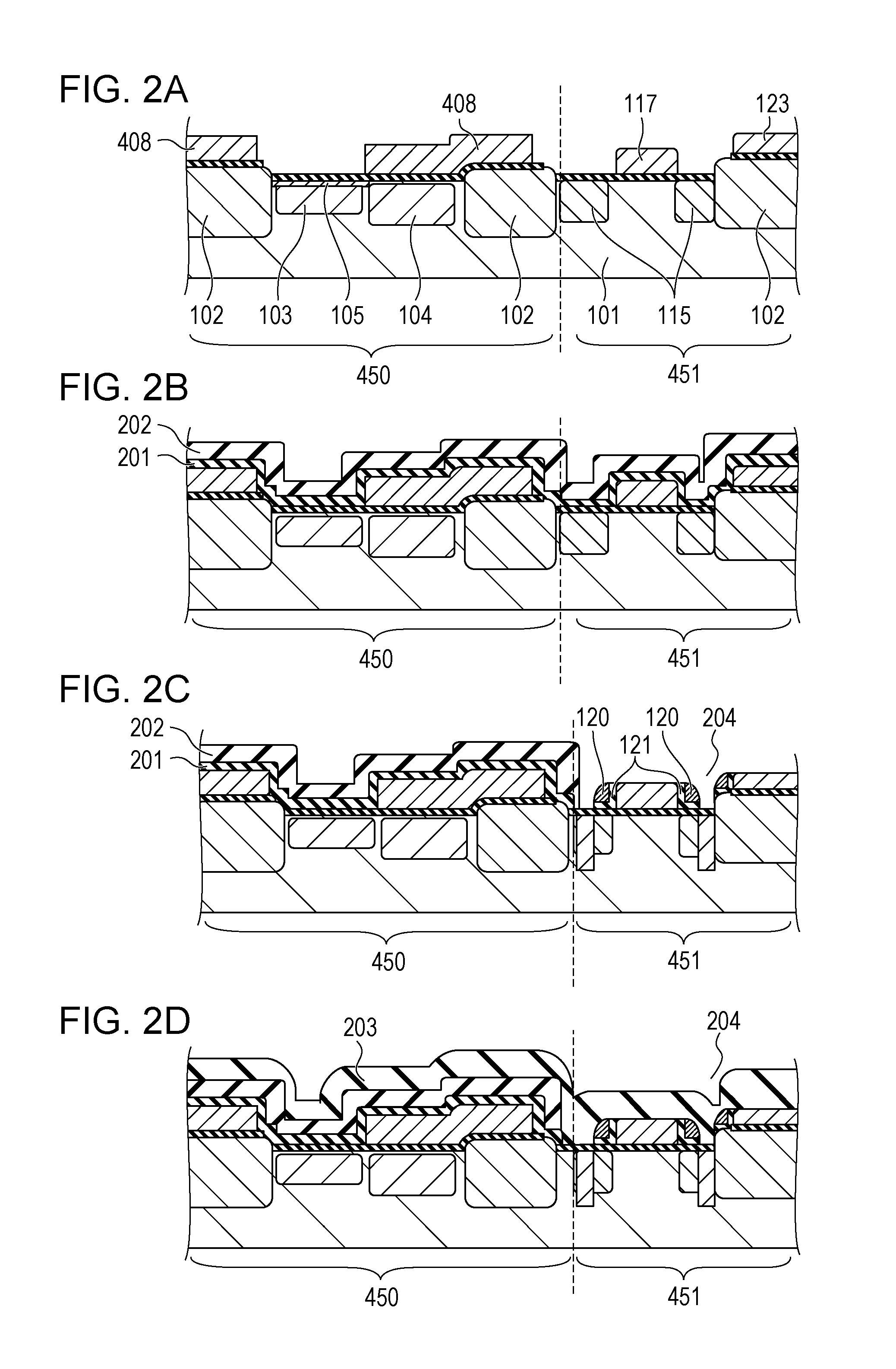
[0020]A solid-state image pickup device according to a first embodiment will be described using FIGS. 1, 4, and 5. FIG. 1 is a schematic sectional view of the solid-state image pickup device according to this embodiment. FIG. 4 illustrates a circuit diagram of four pixels included in the solid-state image pickup device according to this embodiment. FIG. 5 is a schematic plan view corresponding to FIG. 4.

[0021]First, the description will be given of FIG. 4 illustrating a circuit diagram of four pixels of the solid-state image pickup device according to this embodiment and FIG. 5 illustrating a schematic plan view that corresponds to FIG. 4. FIG. 4 illustrates a configuration in which pixels 413 each having a charge holding part are arranged in a 2×2 matrix form. In this embodiment, each pixel 413 includes a photoelectric conversion element 402, a charge holding part 403, a floating diffusion part 404, a power supply part 405, a pixel output part 407, a first gate electrode 408 of a f...

second embodiment

[0037]As in the first embodiment, a solid-state image pickup device according to a second embodiment relates a solid-state image pickup device having light-shielding films. Unlike the first embodiment, the solid-state image pickup device according to this embodiment relates to a solid-state image pickup device having pixels for acquiring image signals and pixels for acquiring focus detection signals in the pixel portion 450. The solid-state image pickup device according to this embodiment will be described using FIGS. 6A to 7.

[0038]FIG. 6A illustrates a circuit diagram of a pixel 713 of the solid-state image pickup device according to this embodiment. In this embodiment, the pixel 413 of the solid-state image pickup device according to the first embodiment illustrated in FIG. 4 is replaced with the pixel 713 illustrated in FIG. 6A. The pixel 713 illustrated in FIG. 6A has a circuitry of a general CMOS solid-state image pickup device. Specifically, the pixel 713 includes a photoelect...


PUM


Abstract

A method for manufacturing a solid-state image pickup device that includes a pixel portion and a peripheral circuit portion, includes: forming a first insulating film in the pixel portion and the peripheral circuit portion, forming a second insulating film above the first insulating film, etching the second insulating film in photoelectric conversion elements, forming a metal film on the etched second insulating film in the photoelectric conversion elements and on the second insulating film in the peripheral circuit portion, and removing the metal film in the peripheral circuit portion and forming light-shielding films from the metal film in the photoelectric conversion elements.

Description

BACKGROUND OF THE INVENTION[0001]1. Field of the Invention[0002]One disclosed aspect of the embodiments relates to methods for manufacturing solid-state image pickup devices. More particularly, one disclosed aspect of the embodiments relates to a technique for forming a light-shielding film in a solid-state image pickup device including pixels having a light-shielding film.[0003]2. Description of the Related Art[0004]Regarding active-pixel solid-state image pickup devices such as complementary metal oxide semiconductor (CMOS) image sensors, configurations have been proposed in which a global electronic shutter function is implemented in pixels and in which pixels for focus detection are additionally included.[0005]The global electronic shutter function refers to a function of starting and terminating accumulation of photoelectric charges at the same timings in a plurality of pixels arranged in a matrix form. In order to perform the global electronic shutter function, each pixel of a...

Claims


Application Information

Patent Timeline
Patent Type & Authority Patents(United States)
IPC IPC(8): H01L21/00
CPCH01L31/18H01L31/02H01L27/14623H01L27/14674
Inventor HASHIMOTO, KOUHEIITAHASHI, MASATSUGU
Owner CANON KK
Why Eureka
Try Eureka