
Method and device for monitoring movement of mirrors in a MEMS device

a technology of mems and mirror, applied in the direction of optics, instruments, optics, etc., can solve the problems of insufficient knowledge of actuation voltage timing to enable the determination of accurate position, inability to measure this parameter in order to overcome the problem at hand, and inability to accurately monitor the position of mirrors

Active Publication Date: 2013-10-08
STMICROELECTRONICS INT NV
View PDF6 Cites 19 Cited by
  • Summary
  • Abstract
  • Description
  • Claims
  • Application Information

AI Technical Summary

Benefits of technology

[0010]It is object of the present invention to provide a device and method for accurately monitoring the position of mirrors in a MEMS device.
[0014]It is yet another object of the present invention to provide an adequate solution for the 180° ambiguity problem associated with in-plain mirrors of MEMS devices.
[0029]The term “establishing at least one counter signal” as used herein should be understood to encompass also application of minimizing algorithms in order to establish the quantities of current / voltage required to offset (eradicate) the measured ripples.

Problems solved by technology

Unfortunately, the knowledge of the actuation voltage timing is usually insufficient to enable determining the accurate position.
Temperature changes, laser power change and other factors contribute to an overall unacceptable error in many cases, e.g. where a MEMS mirror is used for projecting applications that require accuracy of much less than a pixel.
Unfortunately measuring this parameter in order to overcome the problem at hand has been found quite unsatisfactory for a number of reasons among which is the parasitic capacitance involved.
The above methods measure the absolute capacitance but still fail to provide reliable and accurate information regarding to the mirror position because of parasitic capacitance that is inherent to the system.
In addition due to the nature of the electric circle that drives the mirrors, none of the above methods can measure the capacitance throughout the whole scanning cycle.

Method used


Image

  • Method and device for monitoring movement of mirrors in a MEMS device
  • Method and device for monitoring movement of mirrors in a MEMS device
  • Method and device for monitoring movement of mirrors in a MEMS device

Examples


Embodiment Construction

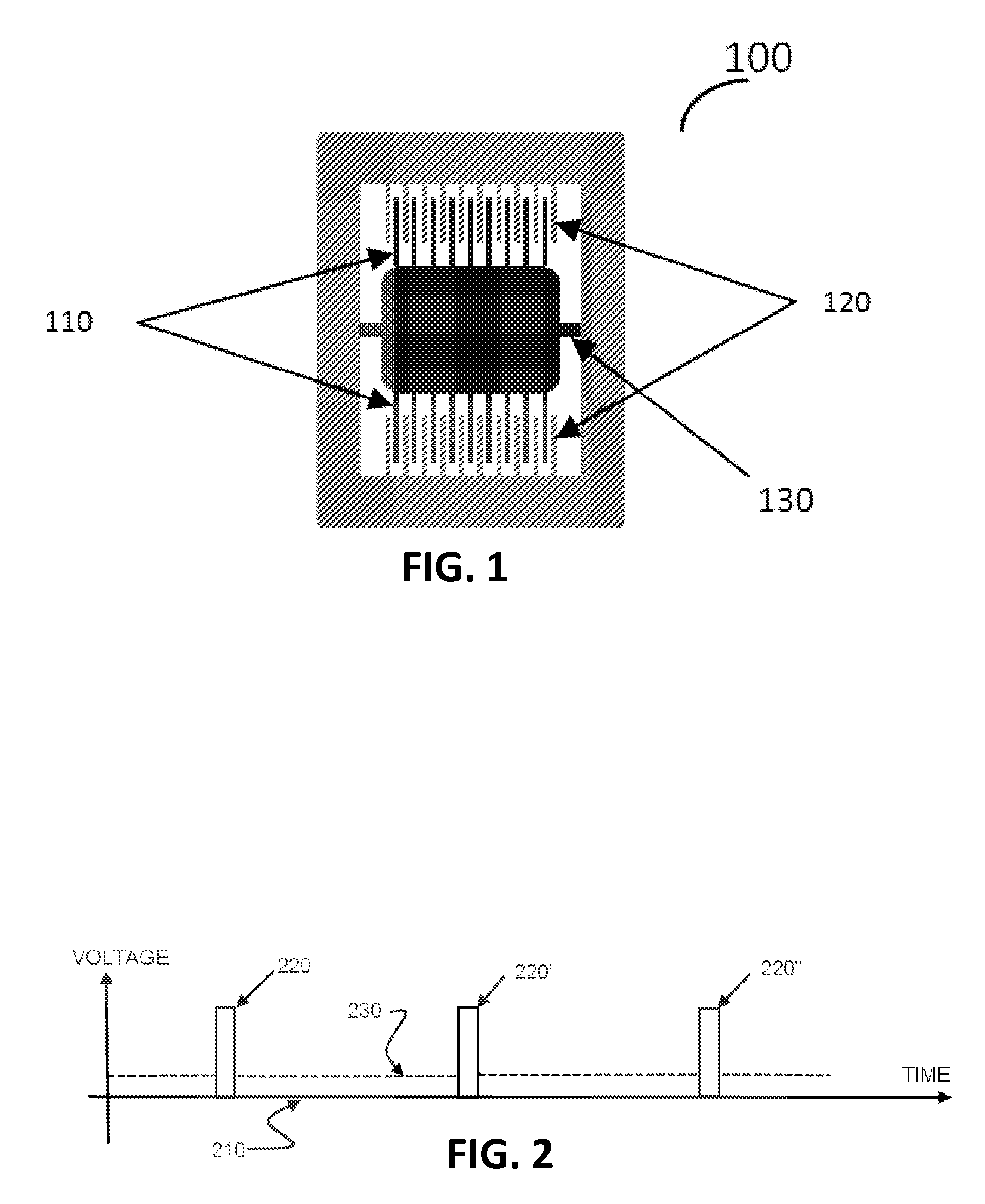
[0067]A better understanding of the present invention may be obtained when the following non-limiting detailed examples are considered in conjunction with the accompanying drawings.

[0068]In order to better understand the various aspects of the present invention, let us consider the following: Equation (1) is derived simply by using the basic definitions of the parameters used:

[0069]I⁡(t)=ⅆQⅆt=ⅆ(CV)ⅆt=C⁢ⅆVⅆt+V⁢ⅆCⅆt(1)

Where:

[0070]I—is the current;

[0071]Q—is the electric charge;

[0072]C—is the capacitance; and

[0073]V—is the voltage.

[0074]In the classic case, the capacitance would remain constant over time, therefore the above equation may be reduced to the following:

[0075]I=C⁢ⅆVⅆt(2)

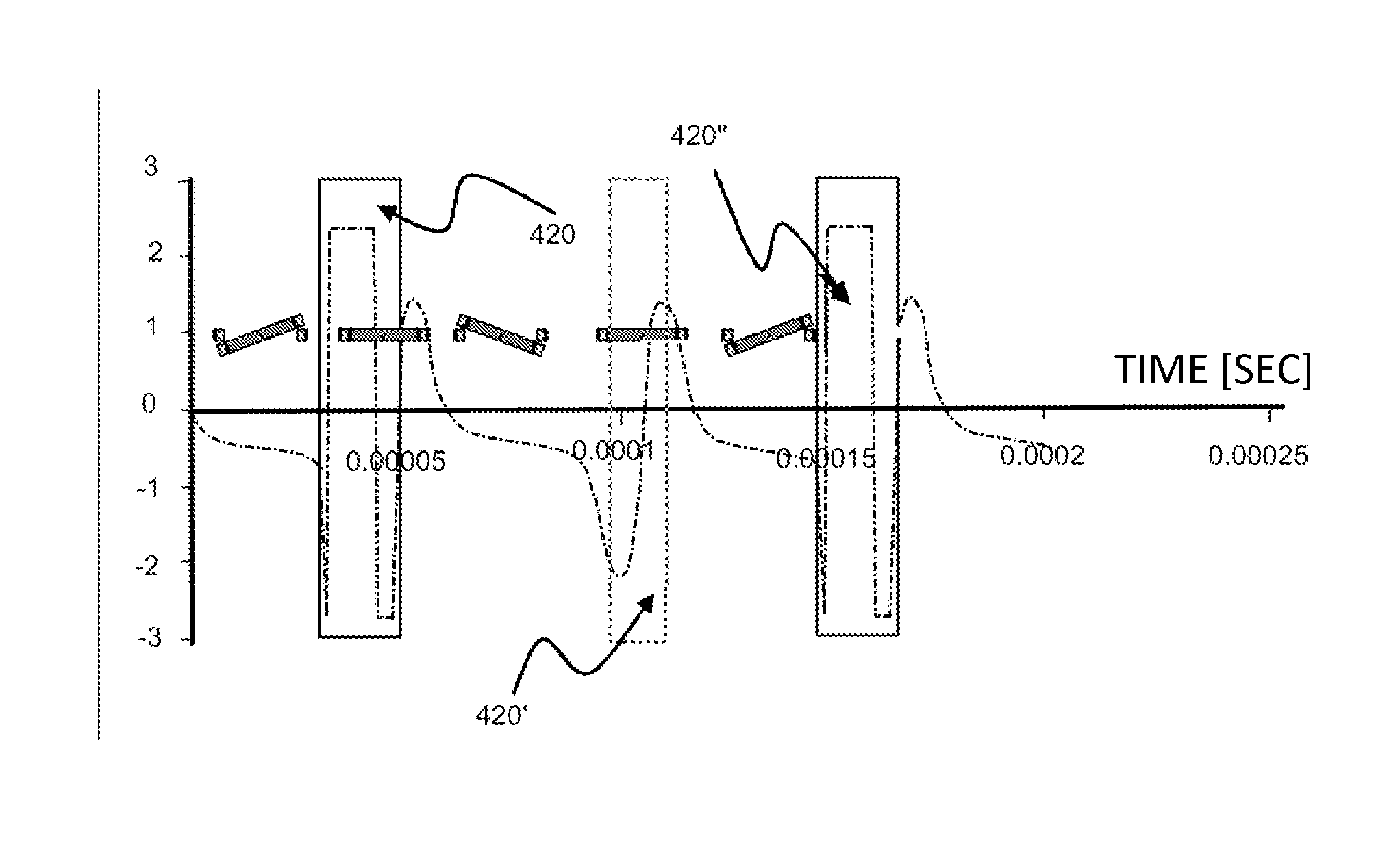
[0076]However, according to a preferred embodiment of the present invention, we are interested in the capacitance change when fixed in time voltage is applied to the system. In this case, equation (1) may be reduced to the following:

[0077]I=ⅆ(CV)ⅆt=V⁢ⅆCⅆt(3)

[0078]In this case the current will indicate the ch...


PUM


Abstract

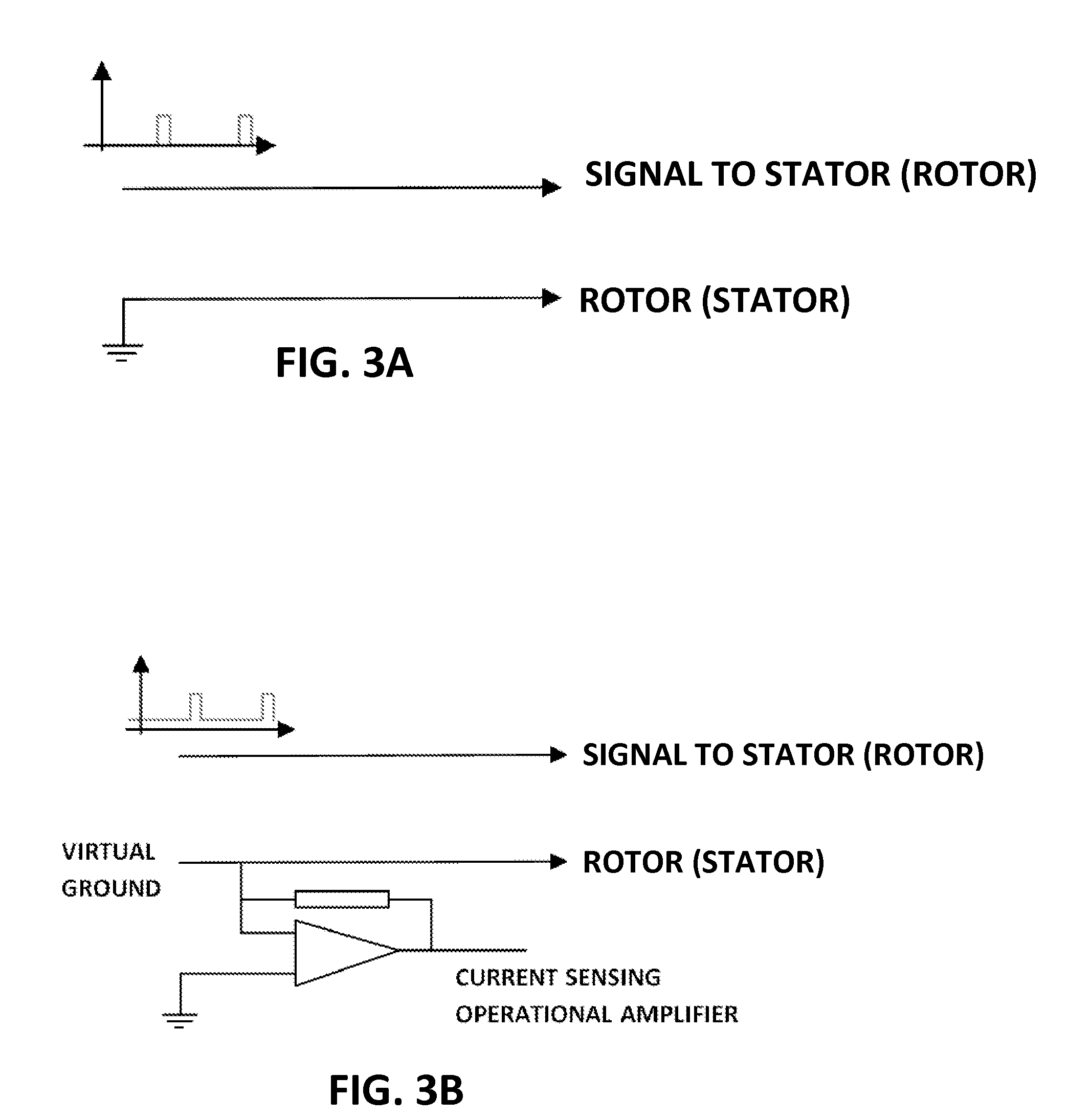
A method for monitoring movement of at least one moving mirror in a MEMS device comprising one or more moving mirrors, and wherein the monitoring is based upon capacitance changes over time in the MEMS device. The method comprises the steps of: if the at least one moving mirror is an in-plain mirror, then: a. providing DC voltage to the MEMS device in addition to a driving voltage required for the movement of that at least one moving mirror; b. measuring current proportional to capacitance changes associated with the movement of the at least one moving mirror; and c. monitoring the movement of the at least one moving mirror based on the measured current. If the at least one moving mirror is a staggered mirror, then: d. measuring a current associated with the movement of the at least one moving mirror; e. identifying a plurality of ripples associated with capacitance changes in the MEMS device over time, in the measured current; and f. monitoring the movement of the at least one moving mirror based on the identified plurality of ripples.

Description

FIELD OF THE INVENTION[0001]The present invention relates to optical systems for scanning or deflecting light beams, and in particularly to MEMS / MOEMS devices which comprise moving reflective elements, such as oscillating mirrors.BACKGROUND OF THE INVENTION[0002]Certain devices such as wafer defect scanners, laser printers, document scanners, projectors and the like make use of a narrow collimated laser beam that usually scan across a flat surface along a straight line path. A typical optical scanning system for this purpose employs a tilting flat mirror to deflect the beam. The tilting micro-mirror serves as a central element in many Micro Electro Mechanical Systems (“MEMS”) devices and / or Micro Opto Electro Mechanical Systems (“MOEMS”) devices. For the convenience of the reader, these devices (i.e. MEMS and / or MOEMS) will be referred to hereinafter throughout the specification and claims as “MEMS” devices. Many of these MEMS devices comprise two types of electro-statically mirrors...

Claims


Application Information

Patent Timeline
Patent Type & Authority Patents(United States)
IPC IPC(8): G02B26/08
CPCG02B26/0841
Inventor GOREN, NIRLUFT, IDOSOURANI, SASON
Owner STMICROELECTRONICS INT NV
Learn More