Resistive memory device having vertical transistors and method for making the same

a technology of resistive memory and transistor, which is applied in the direction of digital storage, semiconductor devices, instruments, etc., can solve the problems of affecting the performance affecting the operation of the memory device, so as to overcome the current drivability and reduce the size of the resistive memory cell

Active Publication Date: 2013-11-05
AVALANCHE TECH
View PDF24 Cites 24 Cited by
  • Summary
  • Abstract
  • Description
  • Claims
  • Application Information

AI Technical Summary

Benefits of technology

[0008]The present invention overcomes the current drivability and punch through current leakage issues associated with the conventional selection transistor while reducing the resistive memory cell size to 4F2 by using a novel cell design that includes an array of vertical selection transistors.

Problems solved by technology

While a memory device employing the selection transistor is more suitable for the random access type of memories, the more complicated structure of the selection transistor means the size of the memory cell will be larger, which translates to a lower cell density.
One way to achieve this is to simply shrink the feature size, F. However, several difficulties can arise when scaling the size of the conventional transistors 92 illustrated in FIG. 1, particularly its channel length, to sizes of a few tens of nanometers.
As the channel length is reduced, there is a propensity for the formation of parasitic conduction paths between source and drain, thereby causing punch through current leakages.
Another obstacle encountered in shrinking the conventional transistors 92 is reduced current drivability caused by the reduced width of the current carrying channel.
This is a significant issue for resistive memory devices, which require higher current to switch their memory state.

Method used


Image

  • Resistive memory device having vertical transistors and method for making the same
  • Resistive memory device having vertical transistors and method for making the same
  • Resistive memory device having vertical transistors and method for making the same

Examples


Embodiment Construction

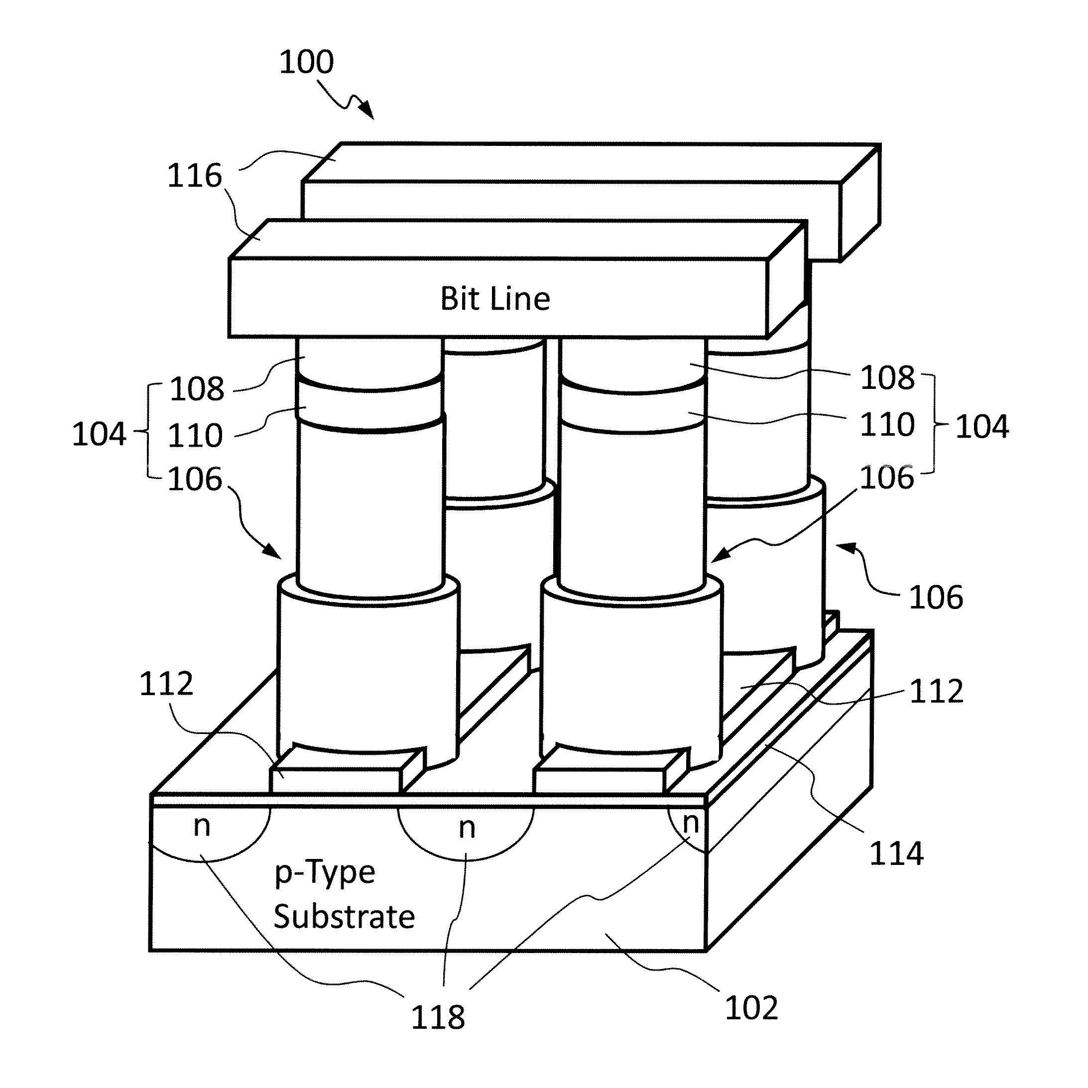
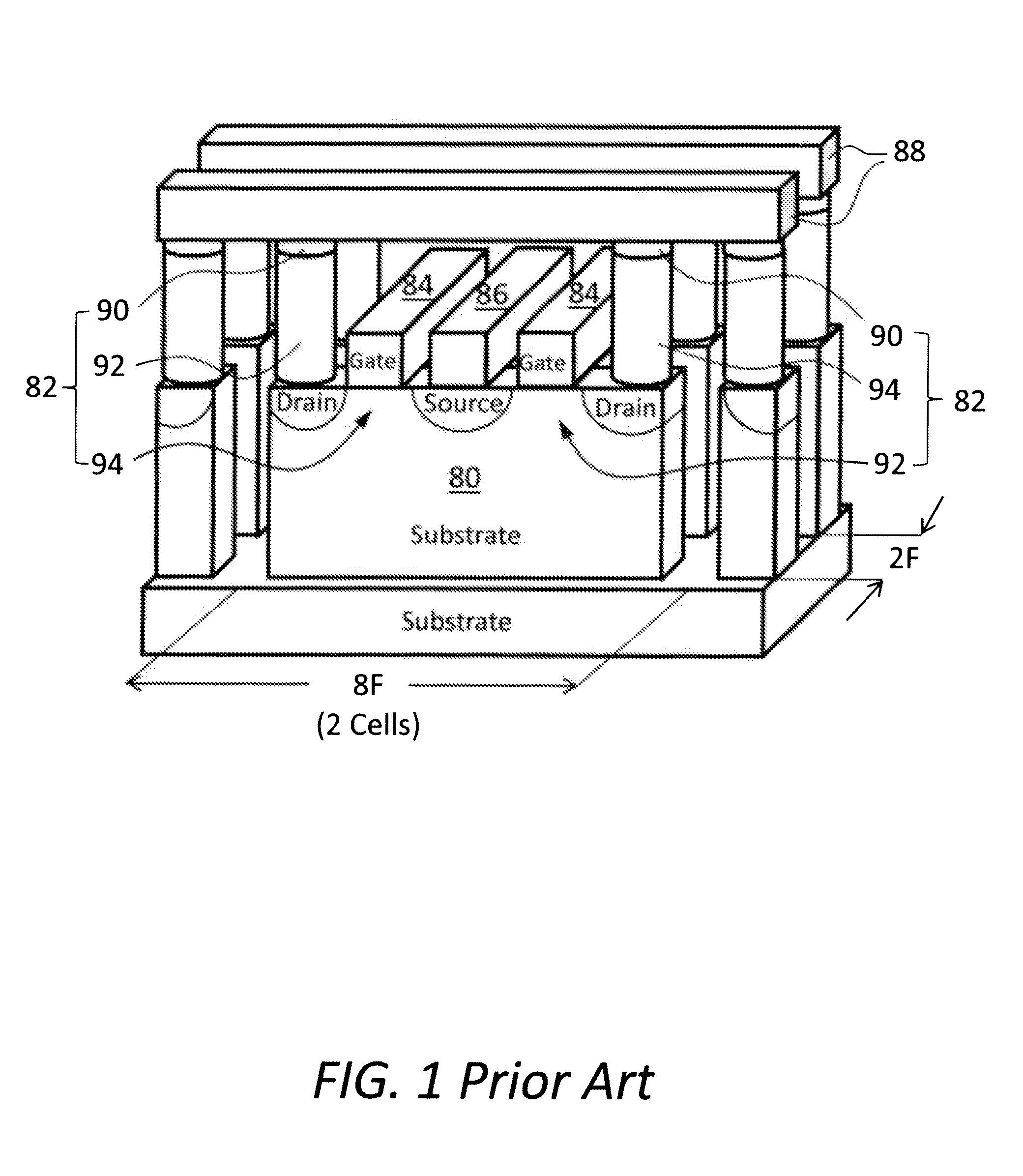
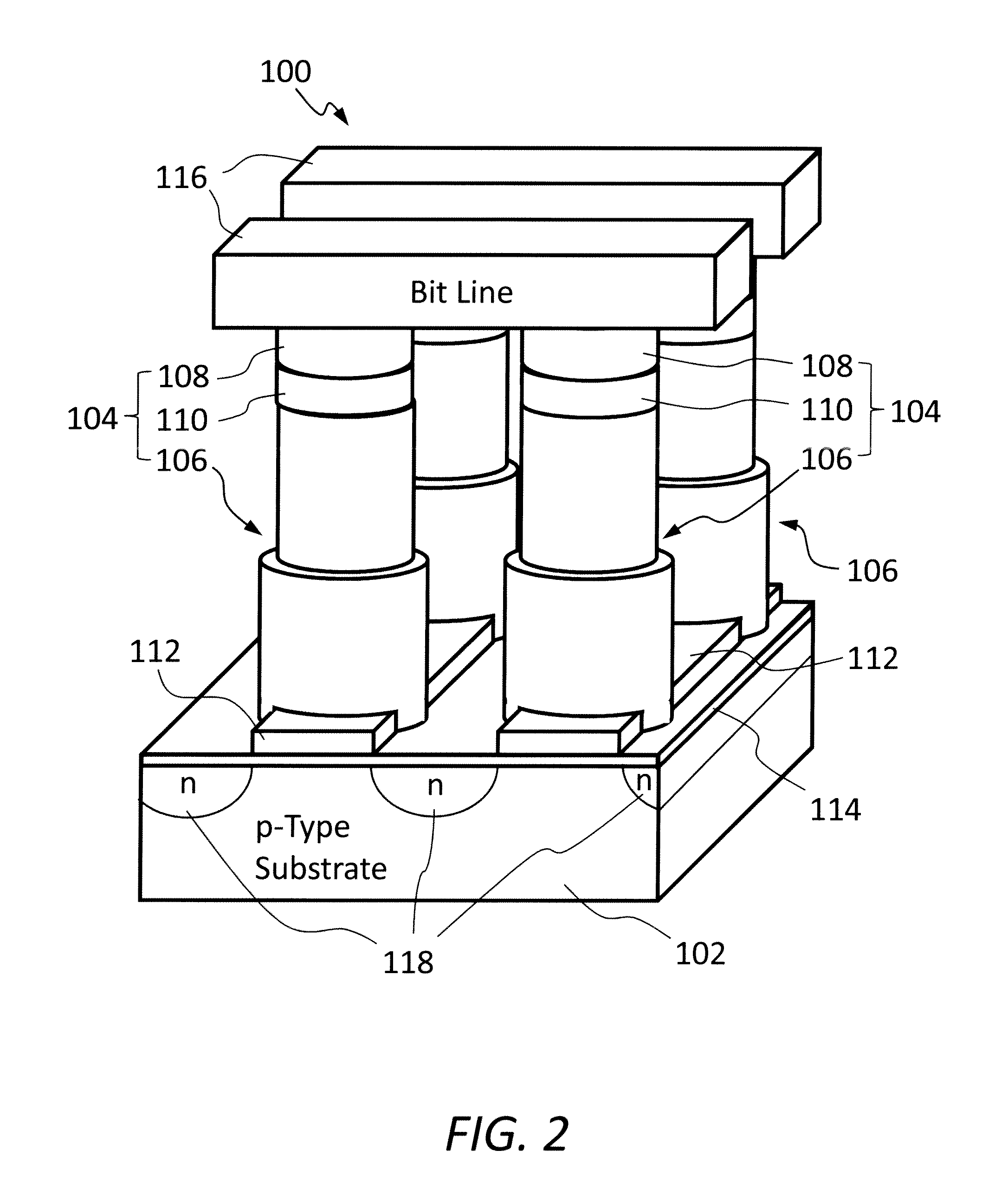
[0021]The present invention overcomes the current drivability and punch through current leakage issues associated with the conventional selection transistor as the feature size shrinks Moreover, the present invention also reduces the resistive memory cell size to 4F2 by using a novel cell design that includes a vertical selection transistor, which has a conductive channel oriented perpendicularly to a substrate therebeneath.

[0022]An embodiment of the present invention as applied to a resistive memory device having an array of memory cells will now be described with reference to FIG. 2. In this drawing, the insulation material separating various elements is omitted for reasons of clarity. The illustrated memory device 100 comprises a semiconductor substrate 102 having a p-type conductivity; a plurality of memory cells 104 formed on the semiconductor substrate 102 in an array, each of the memory cells 104 includes a vertical selection transistor 106, a resistive memory element 108, an...


PUM


Abstract

The present invention relates to resistive memory devices incorporating therein vertical selection transistors and methods for making the same. A resistive memory device comprises a semiconductor substrate having a first type conductivity; a plurality of vertical selection transistors formed on the semiconductor substrate in an array, each of the plurality of vertical selection transistors including a semiconductor pillar protruded from the semiconductor substrate, top region of the semiconductor pillar having a second type conductivity opposite to the first type conductivity provided in the semiconductor substrate; and a gate electrode surrounding the semiconductor pillar with a gate dielectric layer interposed therebetween, the gate electrode being lower in height than the semiconductor pillar; a plurality of contact studs disposed on top of the vertical selection transistors; a plurality of resistive memory elements disposed on top of the contact studs; a plurality of parallel word lines connecting the vertical selection transistors by way of respective gate electrodes, the parallel word lines extending along a first direction; a plurality of parallel bit lines connecting the resistive memory elements, the parallel bit lines extending along a second direction different from the first direction provided in the parallel word lines; and a plurality of parallel source lines with the second type conductivity formed in top regions of the semiconductor substrate in between rows of the semiconductor pillars, wherein the source lines and the top regions of the semiconductor pillars function as source and drain, respectively.

Description

FIELD OF THE INVENTION[0001]The present invention relates to resistive memory devices having an array of vertical selection transistors and method for making the same.BACKGROUND OF THE INVENTION[0002]Resistive memory is a new class of non-volatile memory, which can retain the stored information when powered off. A resistive memory device normally comprises an array of memory cells, each of which includes at least a resistive memory element and a selection element coupled in series between appropriate electrodes. Upon application of an appropriate voltage or current to the resistive memory element, the electrical resistance of the resistive memory element would change accordingly, thereby switching the stored logic in the respective memory cell.[0003]A resistive memory element can be classified into at least one of several known groups based on its resistively switching mechanism. The resistive memory element of Phase Change Random Access Memory (PCRAM) may comprise a phase change ch...

Claims


Application Information

Patent Timeline
Patent Type & Authority Patents(United States)
IPC IPC(8): H01L29/02
CPCH01L27/101H01L27/105H01L27/2463H01L27/2454H01L21/823487H01L45/144H01L45/06H01L45/085H01L45/1233H01L45/146H01L45/147H10B63/34H10B63/80H10N70/245H10N70/231H10N70/8836H10N70/826H10N70/8828H10N70/8833
Inventor SATOH, KIMIHIROHUAI, YIMINGZHANG, JING
Owner AVALANCHE TECH
Why Eureka
Try Eureka