
Memory device having vertical selection transistors with shared channel structure and method for making the same

a technology of vertical selection transistor and channel structure, which is applied in the field of selection transistor in memory devices, can solve the problems of punching through current leakage, affecting the operation of memory devices, etc., and achieves the effect of overcoming current drivability and reducing memory cell siz

Active Publication Date: 2013-05-23
AVALANCHE TECH
View PDF8 Cites 18 Cited by
  • Summary
  • Abstract
  • Description
  • Claims
  • Application Information

AI Technical Summary

Benefits of technology

The present invention is a new memory cell design that solves issues with conventional selection transistors. It uses a novel array of vertical selection transistors that share a common channel, resulting in smaller memory cells and better drivability. The technical effect is improved performance and reduced size of memory cells.

Problems solved by technology

While a memory device employing the selection transistor is more suitable for the random access type of memories, the more complicated structure of the selection transistor means the size of the memory cell will be larger, which translates to a lower cell density.
One way to achieve this is to simply shrink the feature size, F. However, several difficulties can arise when scaling the size of the conventional transistors 92 illustrated in FIG. 1, particularly its channel length, to sizes of a few tens of nanometers.
As the channel length is reduced, there is a propensity for the formation of parasitic conduction paths between source and drain, thereby causing punch through current leakages.
Another obstacle encountered in shrinking the conventional transistors 92 is reduced current drivability caused by the reduced width of the current carrying channel.
This is a significant issue for resistive memory devices, which require higher current to switch their memory state.

Method used


Image

  • Memory device having vertical selection transistors with shared channel structure and method for making the same
  • Memory device having vertical selection transistors with shared channel structure and method for making the same
  • Memory device having vertical selection transistors with shared channel structure and method for making the same

Examples


Embodiment Construction

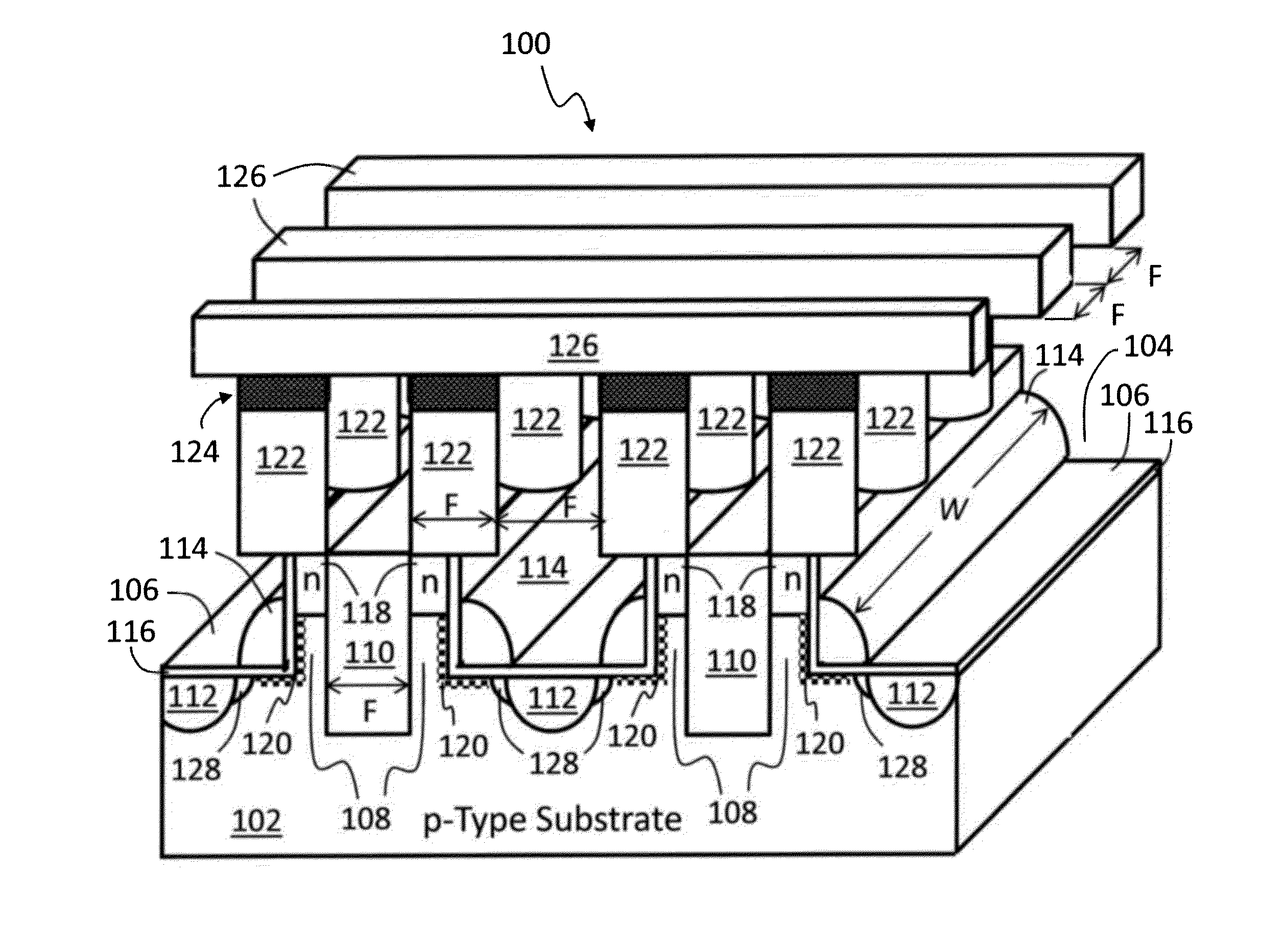
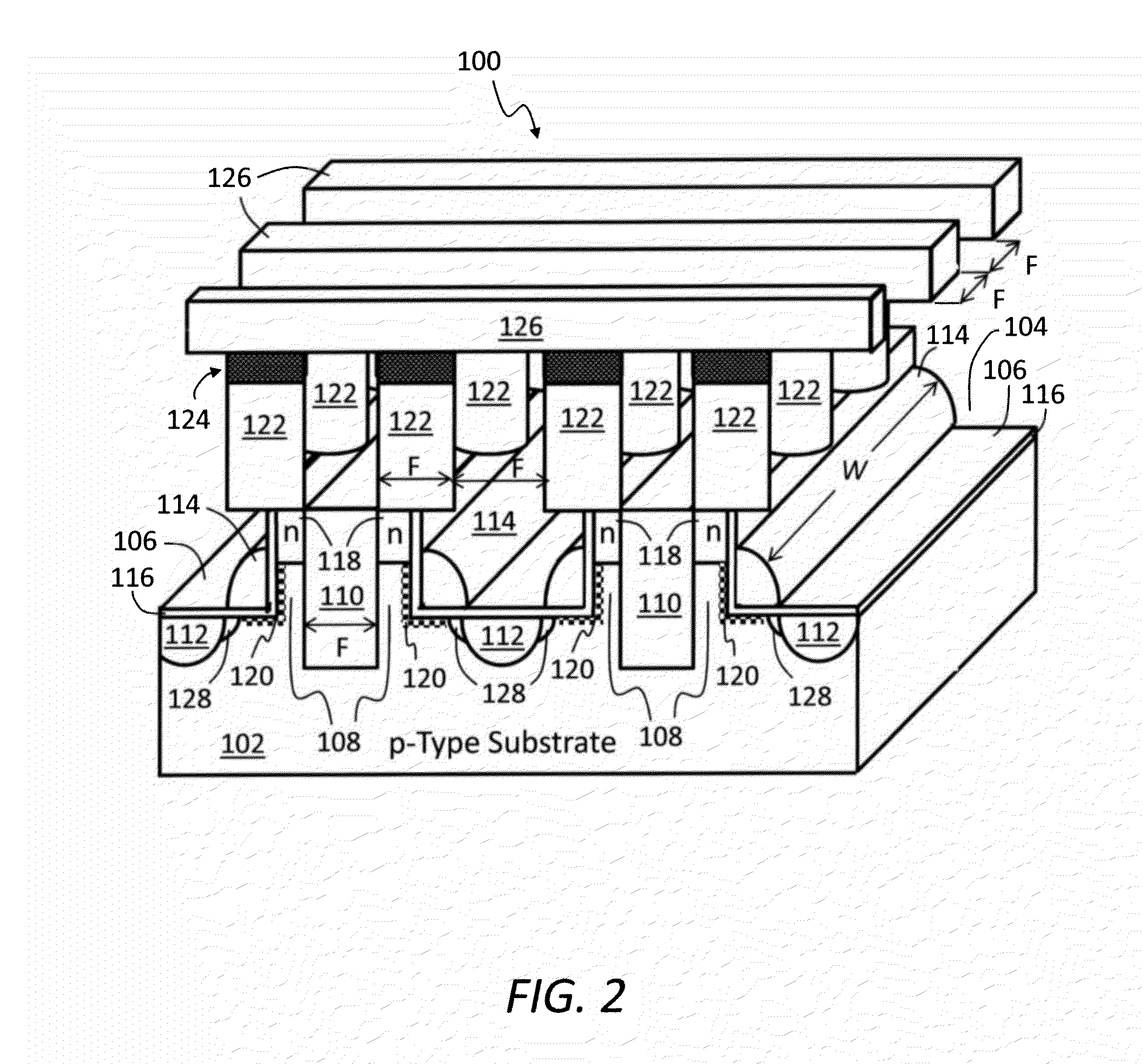
[0020]The present invention overcomes the current drivability and punch through current leakage issues associated with the conventional selection transistor as the feature size shrinks Moreover, the present invention also reduces the resistive memory cell size to 4 F2 by using a novel cell design that includes a plurality of vertical selection transistors sharing a common channel.

[0021]An embodiment of the present invention as applied to a resistive memory device having an array of memory cells will now be described with reference to FIG. 2. In this drawing the insulation material separating various elements is omitted for reasons of clarity. The illustrated memory device 100 comprises a semiconductor substrate 102 having a first type conductivity and a plurality of parallel trenches 104 therein, each of the trenches 104 having a respective one of a plurality of trench bottoms 106 and a respective pair of a plurality of trench sidewalls 108 and being isolated from respective adjacen...


PUM


Abstract

The present invention relates to resistive memory devices incorporating therein vertical selection transistors and methods for making the same. A memory device comprises a semiconductor substrate having a first type conductivity and a plurality of parallel trenches therein; a plurality of parallel common source lines having a second type conductivity opposite to the first type conductivity formed in the trench bottoms; a plurality of parallel gate electrodes formed on the trench sidewalls with a gate dielectric layer interposed therebetween, the gate electrodes being lower in height than the trench sidewalls; and a plurality of drain regions having the second type conductivity formed in top regions of the trench sidewalls, at least two of the drain regions being formed in each of the trench sidewalls and sharing a respective common channel formed in the each of the trench sidewalls and a respective one of the source lines.

Description

RELATED APPLICATIONS[0001]The present application is a continuation-in-part application of U.S. provisional patent application Ser. No. 61 / 562,309, filed Nov. 21, 2011, for MEMORY DEVICE INCLUDING TRANSISTOR ARRAY SHARING COMMON CHANNEL AND PROCESS FOR MAKING THE SAME, by SATOH et al., included by reference herein and for which benefit of the priority date is hereby claimed.FIELD OF THE INVENTION[0002]The present invention relates to Field Effect Transistors (FET), particularly to selection transistors in memory devices.BACKGROUND OF THE INVENTION[0003]Resistive memory is a new class of non-volatile memory, which can retain the stored information when powered off. A resistive memory device normally comprises an array of memory cells, each of which includes at least a resistive memory element and a selection element coupled in series between appropriate electrodes. Upon application of an appropriate voltage or current to the resistive memory element, the electrical resistance of the ...

Claims


Application Information

Patent Timeline
Patent Type & Authority Applications(United States)
IPC IPC(8): H01L45/00H01L21/8239H10B99/00
CPCH01L45/06H01L45/08H01L45/1233H01L45/144H01L27/2463H01L45/147H01L45/16H01L27/2436H01L45/146H10B63/30H10B63/80H10N70/24H10N70/231H10N70/826H10N70/8836H10N70/8828H10N70/8833H10N70/011
Inventor SATOH, KIMIHIROHUAI, YIMINGZHANG, JING
Owner AVALANCHE TECH
Learn More