Semiconductor device and electronic apparatus including the same

Pending Publication Date: 2022-05-19
SONY SEMICON SOLUTIONS CORP
View PDF2 Cites 0 Cited by
  • Summary
  • Abstract
  • Description
  • Claims
  • Application Information

AI Technical Summary

Benefits of technology

[0006]The conventional technology of PTL 1 identified above is capable of reducing a transistor which applies a current necessary for cutting a filament, and therefore is ca

Problems solved by technology

In this case, a problem of a size in

Method used


Image

  • Semiconductor device and electronic apparatus including the same
  • Semiconductor device and electronic apparatus including the same
  • Semiconductor device and electronic apparatus including the same

Examples


first embodiment

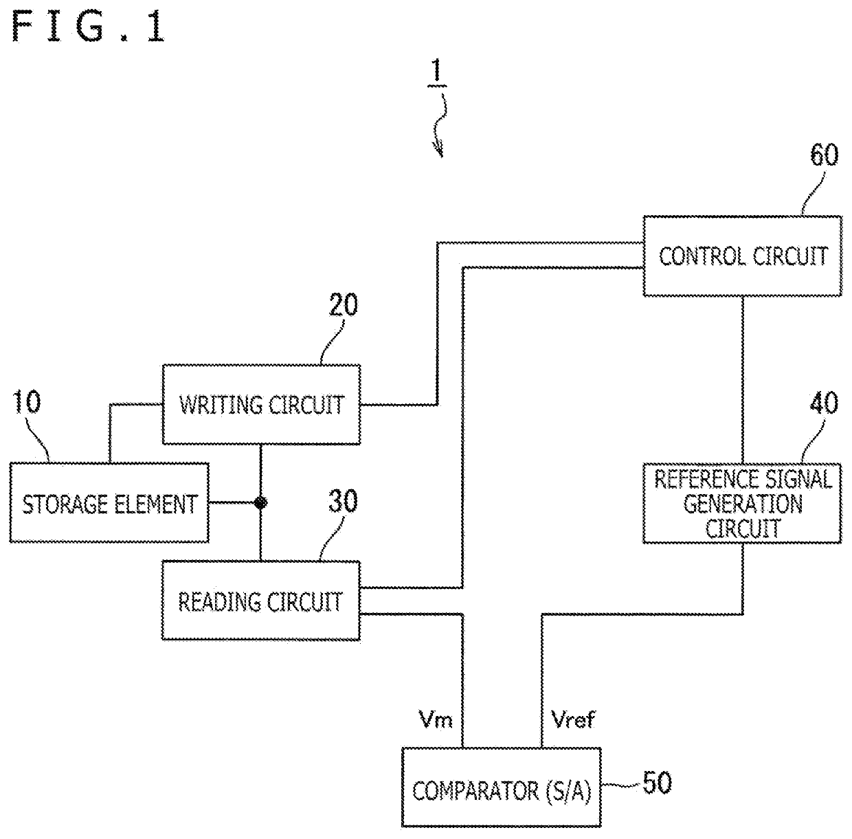
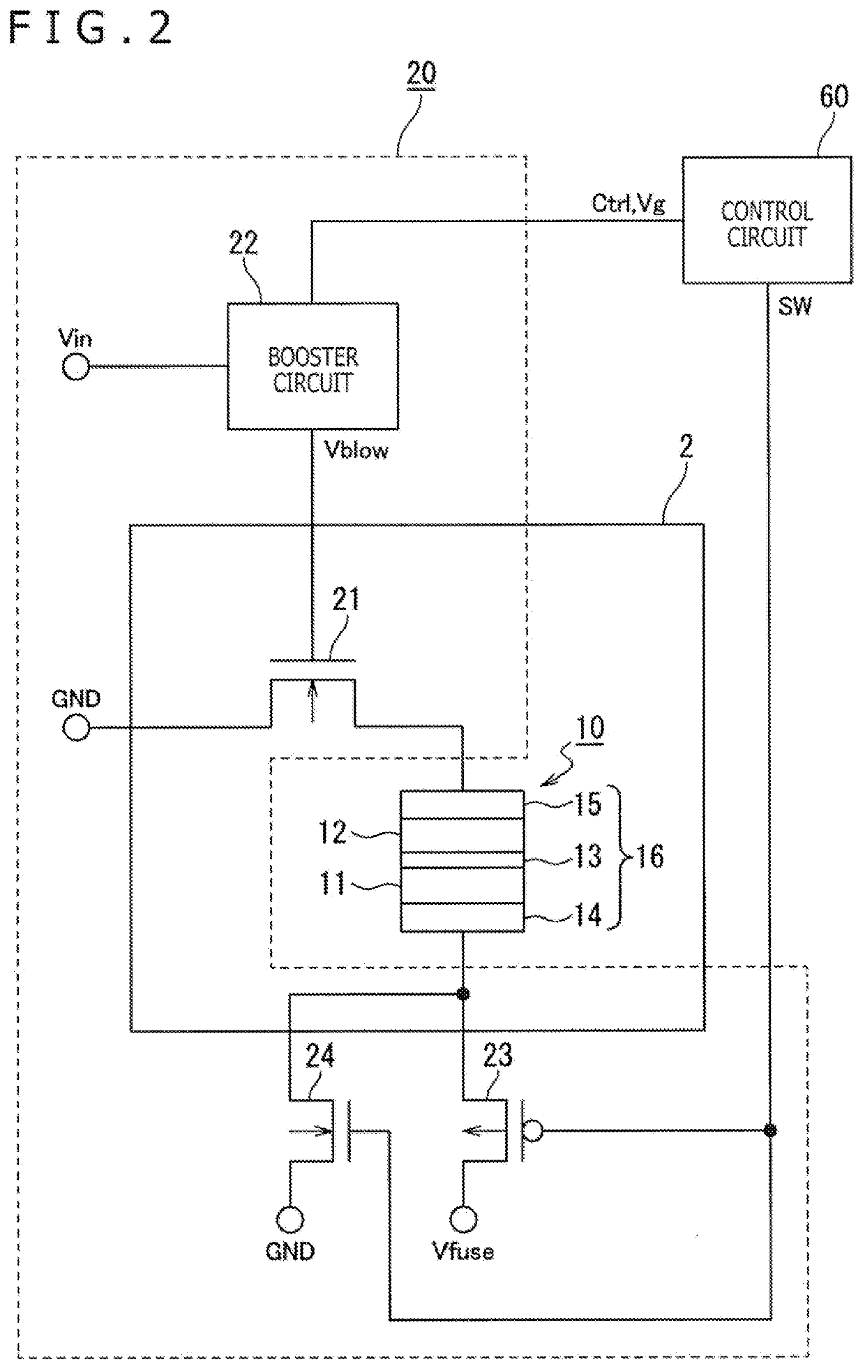
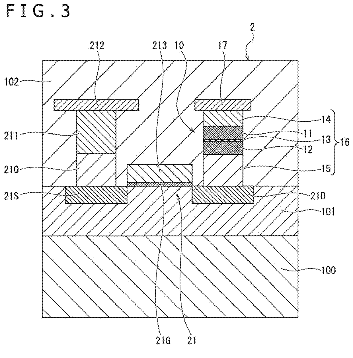
[Configuration Example of Semiconductor Device of First Embodiment]

[0030]Before describing a configuration of a semiconductor device which includes a storage element having a function of an electric fuse according to a first embodiment of the present disclosure, initially briefly touched upon will be a problem which may arise from an increase in capacities of memory cells each including an electric fuse and mounted on a chip such as a semiconductor integrated circuit, for example.

[0031]For example, a method which increases the number of mounted memory cells (mounted capacities) is considered as a simple method for increasing capacities of memory cells mounted on a chip such as a semiconductor integrated circuit. However, each of the memory cells includes a transistor for cutting (breaking) a filament of an electric fuse (hereinafter also referred to as a “blow transistor”). Accordingly, when this method is used to increase the capacities of the memory cells mounted on the chip, an a...

modification 1

[Modification 1 of First Embodiment]

[0136]Described in the above first embodiment has been a configuration which controls the level of the blow current Iblow by changing the level of the blow voltage Vblow applied to the gate electrode 21G of the blow transistor 21 by using the booster circuit 22. Modification 1 of the first embodiment is different from the first embodiment in a point that the level of the blow current Iblow is controlled by changing the level of the writing voltage Vfuse applied to the upper electrode 14 by using a booster circuit 26.

[Configuration of Semiconductor Device 1A According to Modification 1 of First Embodiment]

[0137]FIG. 10 herein is a circuit diagram depicting a configuration example of a part including a writing circuit and a control circuit of a semiconductor device according to modification 1 of the first embodiment.

[0138]For example, as depicted in FIG. 10, a semiconductor device 1A according to the present modification 1 includes a writing circuit...

second embodiment

[0162]Described above in the first embodiment has been the configuration of the semiconductor device 1 including the single memory cell 2. A second embodiment is different from the first embodiment in a point that a semiconductor device 1B includes a memory cell array having a structure where a plurality of the memory cells 2, each of which is a single memory cell depicted in FIG. 2 and described in the first embodiment, are provided in an array arrangement.

[0163]Configuration parts similar to corresponding configuration parts of the first embodiment described above will be hereinafter given similar reference signs to omit repetitive explanation as appropriate, and only different points will be described in detail.

[Configuration of Semiconductor Device 1B]

[0164]FIG. 11 is a diagram depicting an example of an array structure of a memory cell array according to the second embodiment.

[0165]As depicted in FIG. 11, the semiconductor device 1B according to the second embodiment includes a...


PUM


Abstract

A semiconductor device capable of efficiently increasing a capacity of a mounted storage element while achieving space saving, and an electronic apparatus including this semiconductor device are provided. The semiconductor device includes a storage element including a filament that has a first conductive layer, a second conductive layer, and an insulation layer. The first conductive layer and the second conductive layer are stacked with at least the insulation layer interposed between the first conductive layer and the second conductive layer. The filament obtains at least three identifiable resistance states by changing a combination of a state of the first conductive layer, a state of the second conductive layer, and a state of the insulation layer. The semiconductor device further includes a writing unit that produces the at least three identifiable resistance states by applying a blow current to the storage element.

Description

TECHNICAL FIELD[0001]The present disclosure relates to a semiconductor device which includes a storage element capable of storing information by changing a resistance state, and an electronic apparatus including the semiconductor device.BACKGROUND ART[0002]An electric fuse having a function of an OTP (One Time Programmable) memory is conventionally mounted on a chip of a semiconductor integrated circuit or the like included in a semiconductor device. For example, the electric fuse is used as a trimming element for adjusting and correcting characteristics of the semiconductor device, such as performance and power consumption.[0003]A conventional electric fuse causes salicide EM (Electro Migration) or Si melting in a filament of the electric fuse by supplying a predetermined current to the filament. In this manner, a resistance value of the filament is raised to write information to the electric fuse. For example, binary information is stored using “0” for an initial state and “1” for...

Claims


Application Information

Patent Timeline
IPC IPC(8): G11C17/16G11C17/18
CPCG11C17/16G11C17/18H01L27/105G11C17/165H10N50/10H10B99/00
Inventor OKA, MIKIOKANDA, YASUONOGUCHI, KENJI
Owner SONY SEMICON SOLUTIONS CORP
Why Eureka
Try Eureka