Single-polysilicon layer non-volatile memory and operating method thereof

a single-polysilicon, non-volatile technology, applied in the direction of digital storage, solid-state devices, instruments, etc., can solve the problems of increased fabrication cost, prolonged fabrication flow, and inability to reduce so as to achieve the effect of reducing the size of memory cells

Active Publication Date: 2011-12-08
EMEMORY TECH INC
View PDF6 Cites 2 Cited by
  • Summary
  • Abstract
  • Description
  • Claims
  • Application Information

AI Technical Summary

Benefits of technology

[0012]Accordingly, the present invention is directed to a single-polysilicon layer non-volatile memory, in which setting of a select transistor is unnecessary to make a memory array more compact, so that sizes of memory cells can be reduced. To eliminate the select transistor of a memory cell, the electrical array operating methods will be re-designed to fulfil the memory array's purpose accordingly.

Problems solved by technology

During the fabrication process, a plurality of mask processes is performed, so that a fabrication flow is prolonged, and a fabrication cost thereof is increased.
However, in the non-volatile memory disclosed by the U.S. Pat. No. 6,678,190, since one of the P-type metal-oxide semiconductor transistors has to serve as the select transistor, a size of the memory cell cannot be further reduced.
However, the reduced line width often causes the short channel effect, which results in the drop of the threshold voltage (Vt) of the device and poor controlling of the gate voltage (Vg) to the memory cell, and besides, the hot electron effect also occurs, as the channel size is reduced, thus adversely influencing the operation of the memory device.
All the problems cause misjudgement of the data by the memory, thus reducing the reliability of the memory.
Therefore, it can be seen that, how to form a memory with high integration and high reliability has become an urgent problem to be solved.

Method used


Image

  • Single-polysilicon layer non-volatile memory and operating method thereof
  • Single-polysilicon layer non-volatile memory and operating method thereof
  • Single-polysilicon layer non-volatile memory and operating method thereof

Examples


Embodiment Construction

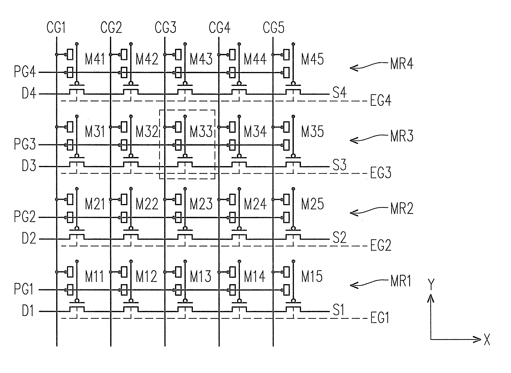
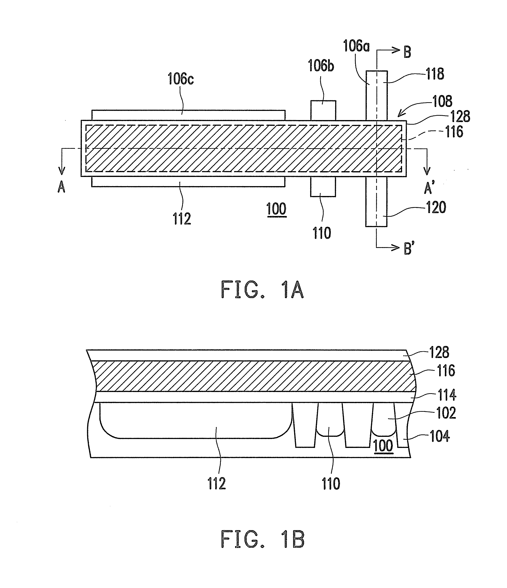
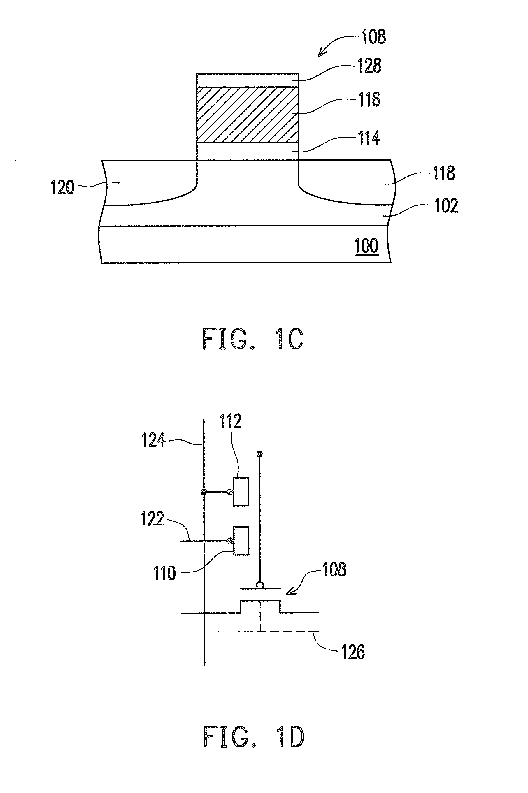
[0044]A single-polysilicon layer non-volatile memory of the present invention is formed by a memory cell array including a plurality of memory cells arranged in rows / columns. First, the memory cell of the present invention is described. FIG. 1A is a top view of a single-polysilicon layer non-volatile memory cell according to an exemplary embodiment of the present invention. FIG. 1B is a cross-sectional view of FIG. 1A along an A-A′ line. FIG. 1C is a cross-sectional view of FIG. 1A along a B-B′ line. FIG. 1D is a simplified circuit diagram of a single-polysilicon layer non-volatile memory cell according to an exemplary embodiment of the present invention.

[0045]Referring to FIG. 1A to FIG. 1D, the non-volatile memory cell is, for example, disposed on a substrate 100, and the substrate 100 is, for example, a silicon substrate. A well region 102 is disposed in the substrate 100, and an isolation structure 104 is disposed in the substrate to define active regions 106a, 106b and 106c. Th...


PUM


Abstract

A single-polysilicon layer non-volatile memory having a floating gate transistor, a program gate and a control gate is provided. The floating gate transistor has a floating gate and a tunneling dielectric layer. The floating gate is disposed on a substrate. The tunneling dielectric layer is disposed between the floating gate and the substrate. The program gate, the control gate and the erase gate are respectively disposed in the substrate under the floating gate separated by the tunneling dielectric layer. Therefore, during a program operation and an erase operation, charges are injected in and expelled out through different regions of the tunneling dielectric layer, so as to increase reliability of the non-volatile memory.

Description

BACKGROUND OF THE INVENTION[0001]1. Field of the Invention[0002]The present invention relates to a semiconductor device. More particularly, the present invention relates to a single-polysilicon layer non-volatile memory string having a single-layer polysilicon floating gate and an operating method thereof.[0003]2. Description of Related Art[0004]When semiconductor fabrication process enters a domain of deep sub-micron, sizes of devices become smaller, so that regarding a memory device, sizes of memory cells thereof become more and more smaller. On the other hand, as data required to be processed and stored by information electronic products (such as computers, mobile phones, digital cameras or personal digital assistants (PDA)) are gradually increased, memory volumes required by these information electronic products become greater. Regarding the situation that the memory size becomes smaller and the memory volume is required to be increased, to fabricate a memory device with a small...

Claims


Application Information

Patent Timeline
Patent Type & Authority Applications(United States)
IPC IPC(8): G11C16/04H01L29/788
CPCG11C16/0433H01L27/11521H01L29/7881H01L29/66825H01L27/11558H10B41/60H10B41/30
Inventor CHEN, HSIN-MINGWANG, SHIH-CHENCHING, WEN-HAOLAI, YEN-HSINYANG, CHING-SUNG
Owner EMEMORY TECH INC
Why Eureka
Try Eureka