Flash memory and method for forming the same

a flash memory and flash technology, applied in the field of flash memory, can solve the problems of increasing the cost of eprom, increasing the difficulty of shrinking the memory cell, increasing manufacturing costs, etc., and achieves the effects of reducing the size of the memory cell, reducing manufacturing costs, and high polysilicon/silicon dioxide etching selectivity

Active Publication Date: 2013-05-30
SHANGHAI HUAHONG GRACE SEMICON MFG CORP
View PDF1 Cites 3 Cited by
  • Summary
  • Abstract
  • Description
  • Claims
  • Application Information

AI Technical Summary

Benefits of technology

[0028]In the flash memory cell, the control gate, the control gate dielectric layer, the floating gate and the floating gate dielectric layer (which correspond to the gate stack of the conventional floating transistor), together with the word line and the word line dielectric layer (which correspond to the gate stack of the conventional select transistor), are formed as an integral structure, so the conventional common doping region is no longer necessary. The size of the memory cell is reduced and the manufacturing costs are decreased.
[0029]Further, the first spacer includes silicon dioxide, which may effectively protect the substance below due to a relatively high polysilicon / silicon dioxide etching selectivity.

Problems solved by technology

However, erasing data in an EPROM requires ultraviolet rays, which raises cost of EPROM.
Therefore, for each data alternation, the whole flash memory needs to be reprogrammed, which is time-wasting.
A common doping region is necessary to realize the connection of the two above-mentioned transistors, which increases difficulty in shrinking the memory cell.
Therefore, the whole EEPROM including a plurality of memory cells may have a relatively large size and occupy a relatively large space, which increase the manufacturing costs.

Method used


Image

  • Flash memory and method for forming the same
  • Flash memory and method for forming the same
  • Flash memory and method for forming the same

Examples


Embodiment Construction

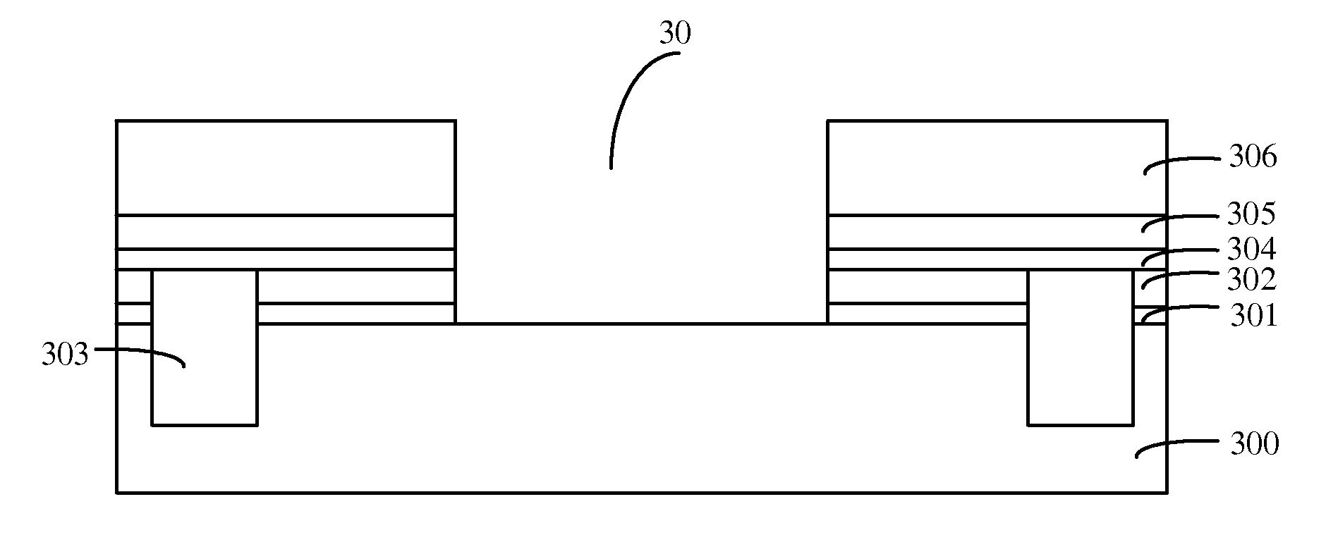
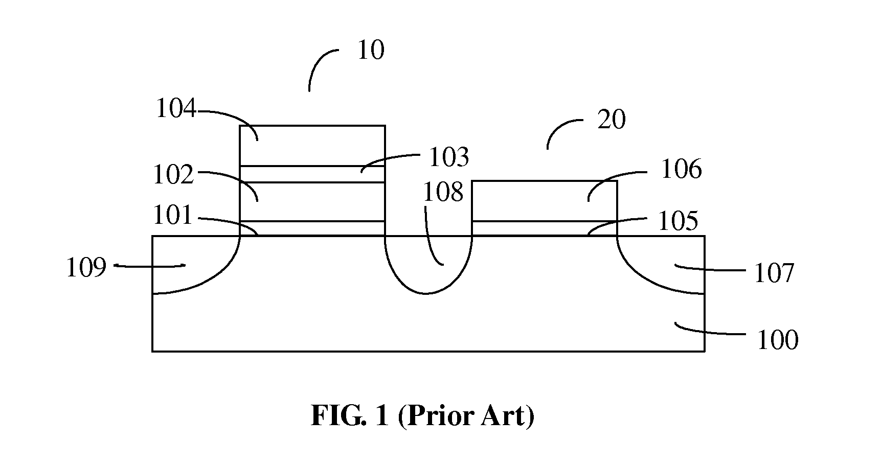
[0034]As described above, the memory cell of the conventional EEPROM includes a storage transistor and a selection transistor which are spaced apart from each other. A common doping region is necessary to realize the connection of the two above-mentioned transistors, which increases difficulty in shrinking the memory cell. Therefore, the whole EEPROM including a plurality of memory cells may have a relatively large size and occupy a relatively large space, which increase the manufacturing costs.

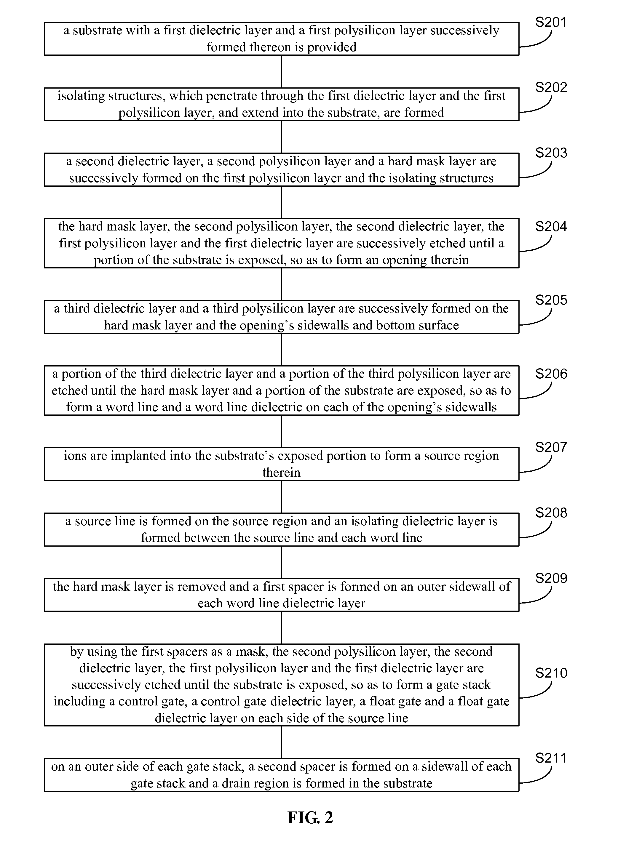
[0035]Therefore, a method for forming a flash memory cell is provided in an embodiment of the present disclosure. The method includes the following process steps: providing a substrate; successively forming a first dielectric layer, a first polysilicon layer, a second dielectric layer, a second polysilicon layer and a hard mask layer on the substrate; successively etching the hard mask layer, the second polysilicon layer, the second dielectric layer, the first polysilicon layer and the first ...


PUM


Abstract

A flash memory cell is provided. The flash memory cell includes: a substrate with a source line thereon; a word line and a word line dielectric layer on each side of the source line; an isolating dielectric layer which isolates the source line from the word line and the word line dielectric layer on each side of the source line; a gate stack on an outer side of each word line dielectric layer, including a floating gate dielectric layer, a floating gate, a control gate dielectric layer and a control gate; a first spacer, disposed on an outer sidewall of each word line dielectric layer and on each control gate; and a source region in the substrate and in contact with the source line. The space may be saved and the costs may be reduced.

Description

CROSS REFERENCE TO RELATED APPLICATIONS[0001]The present application claims priority to Chinese Patent Application No. CN201110379488.X, filed on Nov. 24, 2011, and entitled “FLASH MEMORY AND METHOD FOR FORMING THE SAME”, the entire disclosure of which is incorporated herein by reference.FIELD OF THE DISCLOSURE[0002]The present disclosure generally relates to semiconductor manufacturing, and more particularly, to a flash memory and a method for forming the same.BACKGROUND OF THE DISCLOSURE[0003]Read only memory (ROM), a kind of non-volatile memory, does not lose stored information and data even when power off. Erasable programmable ROM (EPROM) further develops ROM's application into capability of data erasable and rewriteable. However, erasing data in an EPROM requires ultraviolet rays, which raises cost of EPROM. Furthermore, all the programs or data stored in the EPROM are erased indiscriminately in an erasing process even only a portion of them are aimed to be erased. Therefore, ...

Claims


Application Information

Patent Timeline
Patent Type & Authority Applications(United States)
IPC IPC(8): H01L29/788H01L21/336
CPCH01L29/42328H01L27/11521H01L29/66825H10B41/30
Inventor CAO, STEAM
Owner SHANGHAI HUAHONG GRACE SEMICON MFG CORP
Why Eureka
Try Eureka