Magnetic memory device and method for production thereof

a memory device and magnetic technology, applied in semiconductor devices, digital storage, instruments, etc., can solve the problems of too poor endurance to replace sram (static random access memory) and dram (dynamic), and the space between the connecting hole and the first conducting layer can be reduced, so as to reduce the size of the memory cell containing memory elements

Inactive Publication Date: 2005-06-16
SONY CORP
View PDF6 Cites 3 Cited by
  • Summary
  • Abstract
  • Description
  • Claims
  • Application Information

AI Technical Summary

Benefits of technology

[0032] According to the present invention, the lower wiring to be connected to the reading wiring is embedded in the first insulating layer below the first conducting layer and the reading wiring is connected to the lower wiring through the connecting hole which is formed through the second insulating layer in which the first conducting layer has been embedded. The effect of this construction is that the space between the connecting hole and the first conducting layer can be reduced more than in the case where the lower wiring is formed in the same level as the first conducting layer. This offers the advantage of reducing the size of the memory cell containing memory elements.

Problems solved by technology

Flush memory is limited in writing speed to the order of microseconds.
FRAM is also limited in the number of rewriting cycles to 1012 to 1014, that is, it is too poor in endurance to replace SRAM (static random access memory) and DRAM (dynamic random access memory).
Moreover, it presents difficulties in microprocessing of ferroelectric capacitors therein.
Unfortunately, they have the disadvantage that the memory cell has a low resistance of 10-100Ω which leads to a large power consumption per bit for reading.
This disadvantage makes it difficult to realize a large-capacity memory.
However, the proposed means for solution is not necessarily satisfactory.

Method used


Image

  • Magnetic memory device and method for production thereof
  • Magnetic memory device and method for production thereof
  • Magnetic memory device and method for production thereof

Examples


embodiment 1

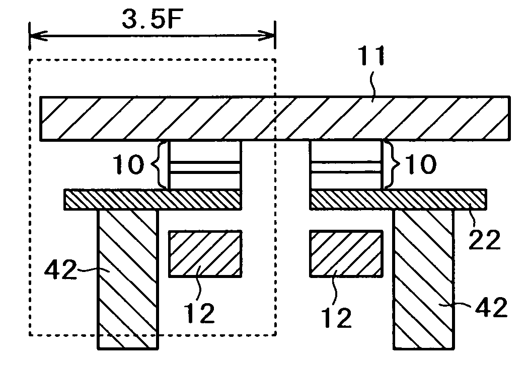
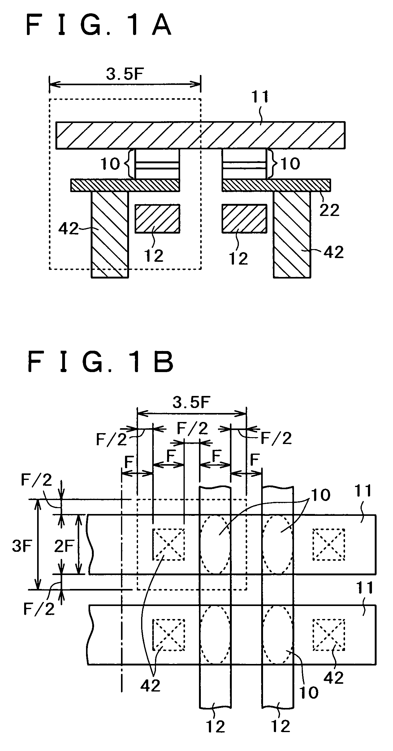
[0081]FIG. 1A is a schematic diagram showing the structure of the MRAM according to this embodiment. FIG. 1B is a schematic plan view of the MRAM according to this embodiment. As shown in these figures, the MRAM is constructed such that the landing pad does not exist at the same level as the word line 12, and the reading wiring 22 is connected to the lower layer wiring (not shown) through the connecting hole 42. This structure makes it possible to bring the connecting hole 42 closer (by F / 2 ) to the word line 12. In this way it is possible to decrease the size in the direction along the bit line 11 to 3.5F.

embodiment 1-1

[0082] The production process will be described with reference to FIGS. 2 to 4. In these figures, MOS transistors etc. under the lower layer wiring are not shown. The same shall apply to other embodiments that follow.

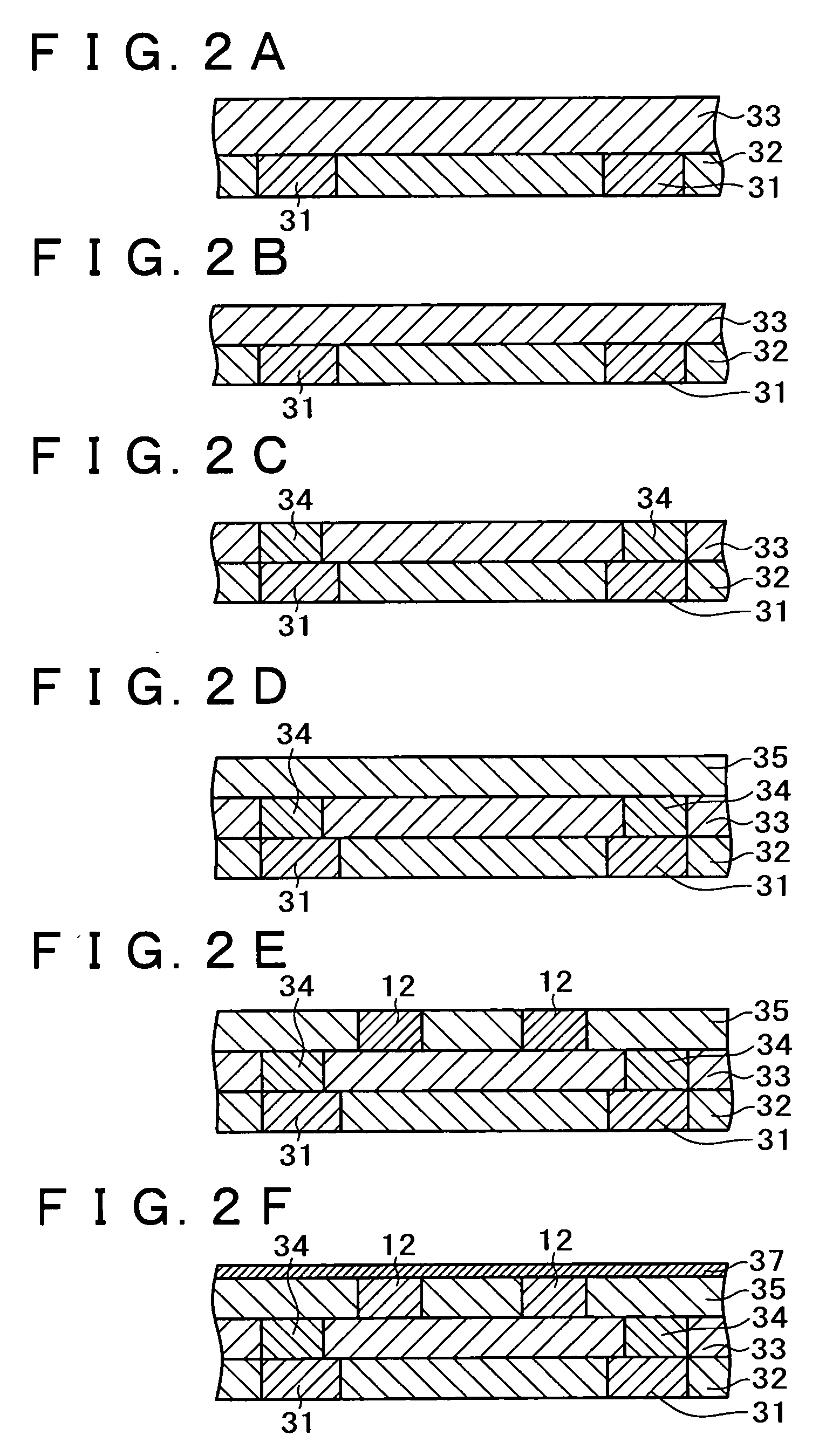
[0083] On the lower layer wiring 31 (600 nm thick) are sequentially formed the HDP film 32 (800 nm thick) and the P-TEOS film 33 (1200 nm thick), as shown in FIG. 2A. The HDP film is a silicon oxide film formed by high-density plasma CVD. The P-TEOS film is a silicon oxide film formed from plasma tetraethyl orthosilicate by reduced pressure CVD. Then, CMP (chemical mechanical polishing) is performed such that an insulting film (700 nm thick) is left on the lower layer wiring 31, as shown in FIG. 2B.

[0084] A connecting hole (not shown) for electrical connection to the lower layer wiring 31 is formed by lithography and etching. In this hole is deposited a tungsten film by CVD. (This tungsten film is referred to as W-CVD hereinafter.) Finally, CMP is performed. In this w...

embodiment 1-2

[0094] The production process will be described with reference to FIGS. 5 to 7.

[0095] First, a lower layer metal wiring 31 (600 nm) is formed. On this layer are sequentially deposited the HDP film 32 (800 nm thick) and the P-TEOS film 33 (1200 nm thick), as shown in FIG. 5A. CMP is performed such that an insulting film (700 nm thick) is left on the lower layer wiring 31, as shown in FIG. 5B.

[0096] The P-SiN film (50 nm thick) (not shown) and the P-TEOS film 35 (400 nm thick) are sequentially deposited, as shown in FIG. 5C. Etching is performed on the P-TEOS film 35 and the P-SiN film through a photoresist film (not shown) as the mask, so that a wiring groove is formed. In this wiring groove are sequentially deposited Ta / TaN / Cu seed layers by sputtering (not shown). The wiring groove is filled with Cu plating. The surface of the wiring groove is planarized by CMP, and the word line 12 is formed, as shown in FIG. 5D. The P-SiN film 37 (50 nm thick) is deposited, as shown in FIG. 5E....


PUM


Abstract

A magnetic memory device in which the memory cell of MRAM is reduced in size, and a method for producing the magnetic memory device are provided. The lower wiring is formed below the word line. The connecting hole and the plug connected to it are provided. The reading wiring and the lower layer wiring are connected through this plug. Alternatively, the local wiring is provided in the connecting hole and the reading wiring and the lower layer wiring are connected. In this way it is possible to form the connecting hole close to the word line, and hence it is possible to reduce the cell size in the direction along the bit line.

Description

BACKGROUND OF THE INVENTION [0001] The present invention relates to a magnetic memory device and a method for production thereof. The magnetic memory device is a magnetic random access memory (MRAM) of nonvolatile type consisting of memory elements each having a magnetization pinned layer in which the direction of magnetization is pinned and a magnetic layer in which the direction of magnetization is variable, with one laid on top of the other. [0002] The recent wide spread of information and communications equipment, particularly personal small ones such as portable terminals, requires their constituents (such as memory elements and logic elements) to have improved performance, including high integration, high speed, and low power consumption. [0003] Particularly, non-volatile memory is regarded as indispensable in the age of ubiquitous computing because it preserves personal important information in case of dead battery and network failure or server breakdown. Recent portable equi...

Claims


Application Information

Patent Timeline
Patent Type & Authority Applications(United States)
IPC IPC(8): H01L27/105G11C11/14G11C11/16H01L21/8246H01L27/22H01L43/08
CPCB82Y10/00H01L27/228G11C11/16H10B61/22
Inventor MOTOYOSHI, MAKOTO
Owner SONY CORP
Why Eureka
Try Eureka