
Memory

a memory and memory technology, applied in the field of memory, can solve the problem of disadvantageous increase in and achieve the effect of reducing the size of the memory cell

Active Publication Date: 2007-01-25
SEMICON COMPONENTS IND LLC
View PDF5 Cites 4 Cited by
  • Summary
  • Abstract
  • Description
  • Claims
  • Application Information

AI Technical Summary

Benefits of technology

[0008] The present invention has been proposed in order to solve the aforementioned problem, and an object of the present invention is to provide a memory capable of reducing the memory cell size.

Problems solved by technology

In the conventional mask ROM shown in FIG. 8, however, the memory cell size is disadvantageously increased due to the transistors 103 provided in correspondence to the respective memory cells 104.

Method used


Image

  • Memory
  • Memory
  • Memory

Examples


Embodiment Construction

[0035] An embodiment of the present invention is now described with reference to the drawings. In the following description of the embodiment, the present invention is applied to a mask ROM utilizing a diode matrix (hereinafter referred to as a diode ROM) as an exemplary memory.

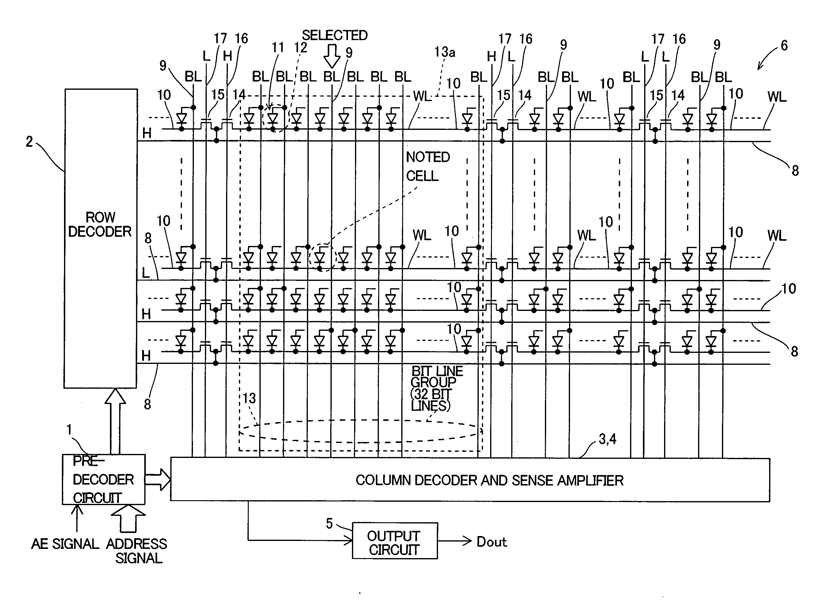
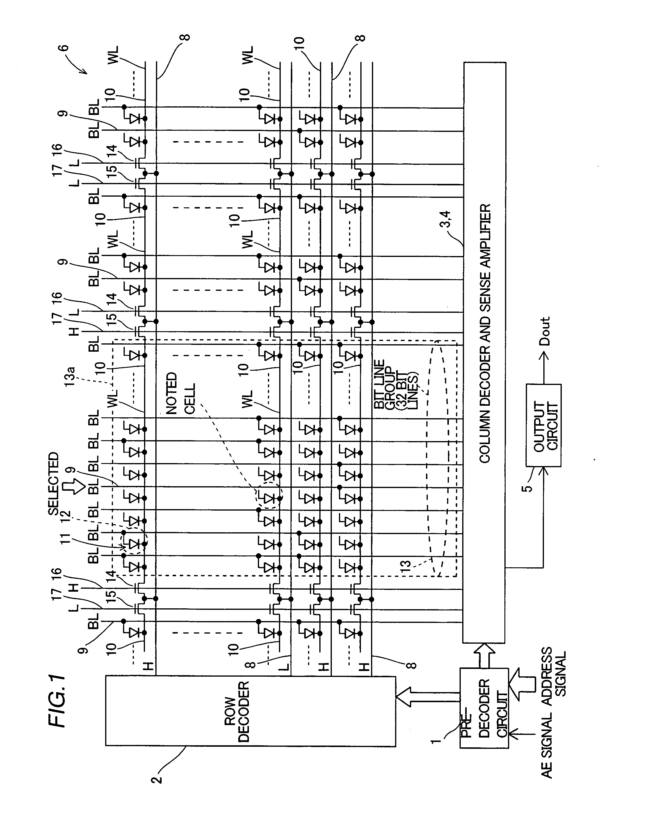
[0036]FIG. 1 is a circuit diagram showing the structure of the diode ROM according to the embodiment of the present invention. The overall structure of the diode ROM according to the embodiment of the present invention is now described with reference to FIG. 1.

[0037] As shown in FIG. 1, the diode ROM according to this embodiment comprises a predecoder circuit 1, row decoders 2, column decoders 3, sense amplifiers 4, output circuits 5 and a memory cell array 6. The predecoder circuit 1 is so formed as to receive an external address signal and an external address enable (AE) signal thereby outputting a predecoding signal for selecting a prescribed address to each row decoder 2, each column decoder 3 and each ...


PUM


Abstract

A memory capable of reducing the memory cell size is provided. This memory comprises a plurality of memory cells including diodes, a plurality of bit lines and an n-type impurity region arranged to intersect with the bit lines for functioning as cathodes of the diodes included in the memory cells and a word line. The n-type impurity region is divided every bit line group formed by a prescribed number of bit lines.

Description

BACKGROUND OF THE INVENTION [0001] 1. Field of the Invention [0002] The present invention relates to a memory, and more particularly, it relates to a memory such as a mask ROM. [0003] 2. Description of the Background Art [0004] A mask ROM disclosed in Japanese Patent Laying-Open No. 5-275656 (1993) is generally known as an exemplary memory. [0005]FIG. 8 is a plane layout diagram showing the structure of a conventional contact-mask ROM. Referring to FIG. 8, a plurality of word lines 101 and a plurality of bit lines 102 are arranged to intersect with each other in the conventional contact-mask ROM. Memory cells 104 formed by single transistors 103 respectively are arranged on positions corresponding to the intersections between the plurality of word lines 101 and the plurality of bit lines 102 respectively. The word lines 101 are formed on a substrate (not shown) through gate insulating films (not shown) of the transistors 103. These word lines 101 function also as gate electrodes of ...

Claims


Application Information

Patent Timeline
Patent Type & Authority Applications(United States)
IPC IPC(8): G11C17/00
CPCG11C17/06H01L27/11253H01L27/112H10B20/38H10B20/00
Inventor YAMADA, KOUICHI
Owner SEMICON COMPONENTS IND LLC
Learn More