Methods for bonding semiconductor structures involving annealing processes, and bonded semiconductor structures and intermediate structures formed using such methods

a technology of annealing process and semiconductor structure, which is applied in the direction of semiconductor/solid-state device details, semiconductor devices, electrical apparatus, etc., can solve the problems of prone to mechanical failure or electrical failure, less partial melting of metal materials, and undesirable direct bonding processes

Inactive Publication Date: 2014-05-06
SONY SEMICON SOLUTIONS CORP
View PDF8 Cites 104 Cited by
  • Summary
  • Abstract
  • Description
  • Claims
  • Application Information

AI Technical Summary

Problems solved by technology

For example, some direct metal-to-metal bonding methods are carried out at relatively high temperatures resulting in at least partial melting of the metal material at the bonding interface.
Such direct bonding processes may be undesirable for use in bonding processed semiconductor structures that include one or more device structures, as the relatively high temperatures may adversely affect the earlier formed device structures.
Direct metal-to-metal bonds between active conductive features in semiconductor structures may, in some instances, be prone to mechanical failure or electrical failure after a period of time even though an acceptable direct metal-to-metal bond may be initially established between the conductive features of the semiconductor structures.

Method used


Image

  • Methods for bonding semiconductor structures involving annealing processes, and bonded semiconductor structures and intermediate structures formed using such methods
  • Methods for bonding semiconductor structures involving annealing processes, and bonded semiconductor structures and intermediate structures formed using such methods
  • Methods for bonding semiconductor structures involving annealing processes, and bonded semiconductor structures and intermediate structures formed using such methods

Examples


embodiment 1

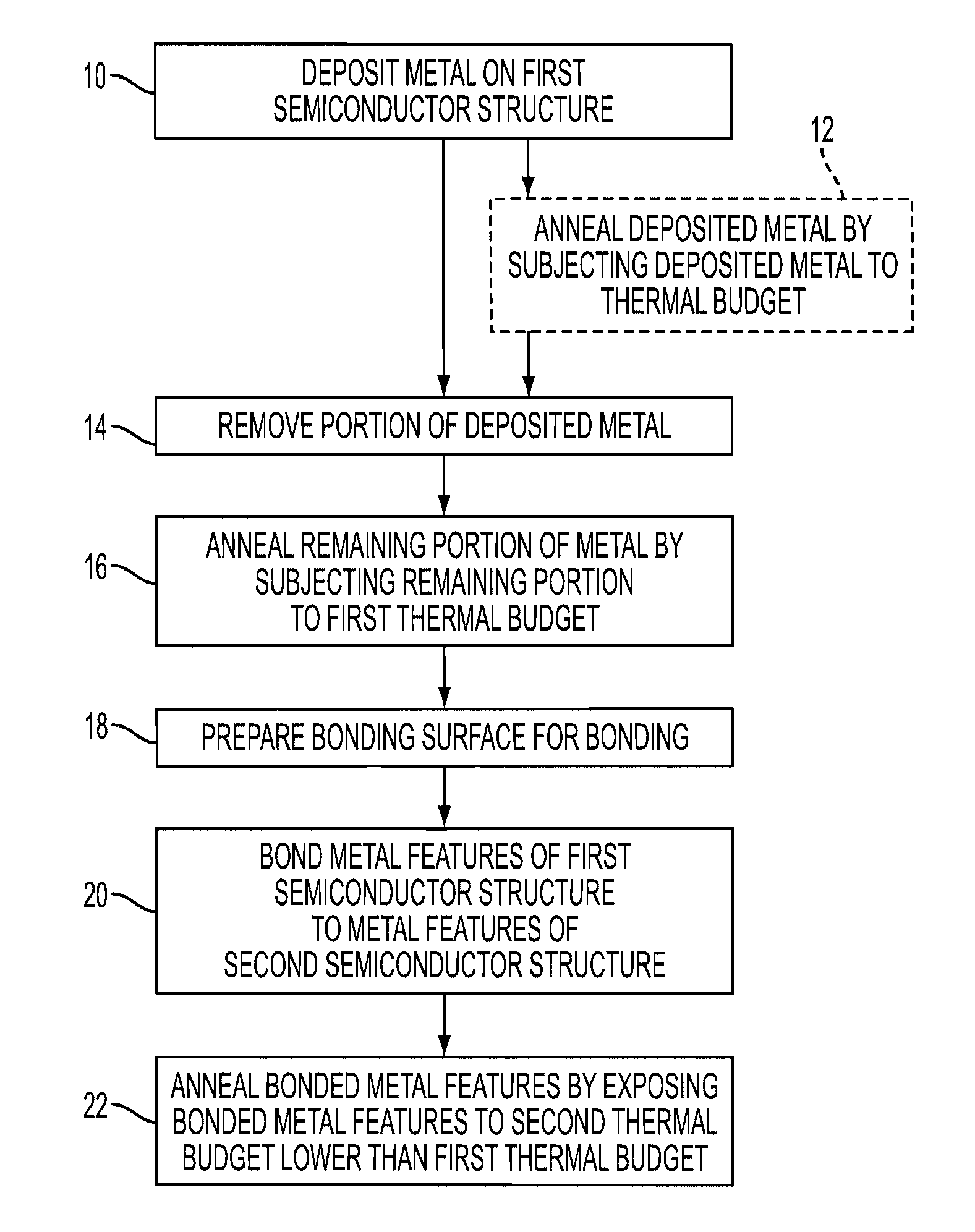
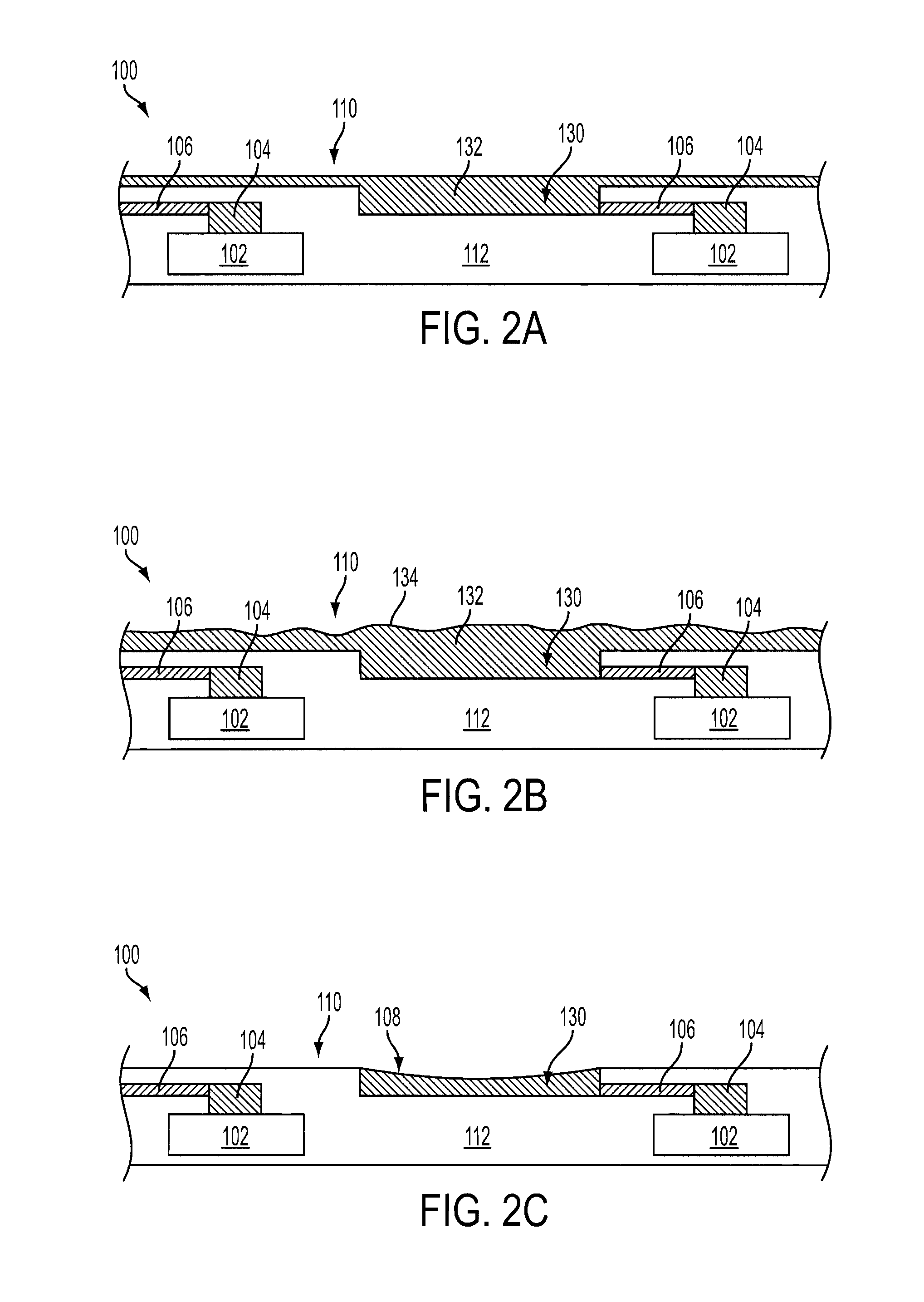
[0123]A method of directly bonding a first semiconductor structure to a second semiconductor structure, comprising: depositing metal over a first semiconductor structure; removing a portion of the metal deposited over the first semiconductor structure; subjecting a remaining portion of the metal deposited over the first semiconductor structure to a first thermal budget and annealing the remaining portion of the metal deposited over the first semiconductor structure; directly bonding at least one metal feature of the first semiconductor structure comprising the remaining portion of the metal deposited over the first semiconductor structure to at least one metal feature of a second semiconductor structure to form a bonded metal structure comprising the at least one metal feature of the first semiconductor structure and the at least one metal feature of the second semiconductor structure; and subjecting the bonded metal structure to a second thermal budget and annealing the bonded meta...

embodiment 2

[0124]The method of Embodiment 1, wherein subjecting the remaining portion of the metal deposited over the first semiconductor structure to the first thermal budget and annealing the remaining portion of the metal deposited over the first semiconductor structure comprises subjecting the remaining portion of the metal to a first average annealing temperature over a first annealing time period, and wherein subjecting the bonded metal structure to a second thermal budget and annealing the bonded metal structure comprises subjecting the bonded metal structure to a second average annealing temperature over a second annealing time period.

embodiment 3

[0125]The method of Embodiment 2, wherein the first average annealing temperature is higher or equal than the second average annealing temperature.


PUM

PropertyMeasurementUnit
thicknessaaaaaaaaaa
temperatureaaaaaaaaaa

Abstract

Methods of bonding together semiconductor structures include annealing metal of a feature on a semiconductor structure prior to directly bonding the feature to a metal feature of another semiconductor structure to form a bonded metal structure, and annealing the bonded metal structure after the bonding process. The thermal budget of the first annealing process may be at least as high as a thermal budget of a later annealing process. Additional methods involve forming a void in a metal feature, and annealing the metal feature to expand the metal of the feature into the void. Bonded semiconductor structures and intermediate structures are formed using such methods.

Description

TECHNICAL FIELD[0001]Embodiments of the present disclosure relate to methods of bonding together semiconductor structures, and to bonded semiconductor structures and intermediate structures formed using such methods.BACKGROUND[0002]The three-dimensional (3D) integration of two or more semiconductor structures can produce a number of benefits to microelectronic applications. For example, 3D integration of microelectronic components can result in improved electrical performance and power consumption while reducing the area of the device footprint. See, for example, P. Garrou et al., “The Handbook of 3D Integration,” Wiley-VCH (2008).[0003]The 3D integration of semiconductor structures may take place by the attachment of a semiconductor die to one or more additional semiconductor dies (i.e., die-to-die (D2D)), a semiconductor die to one or more semiconductor wafers (i.e., die-to-wafer (D2W)), as well as a semiconductor wafer to one or more additional semiconductor wafers (i.e., wafer-t...

Claims


Application Information

Patent Timeline
Patent Type & Authority Patents(United States)
IPC IPC(8): H01L21/30H01L23/00H01L21/46H01L21/00
CPCH01L2924/01074H01L2224/05571H01L2224/05647H01L24/80H01L2224/80357H01L24/05H01L24/08H01L2224/08147H01L2224/80896H01L21/187H01L24/01H01L2224/0903H01L2224/80895H01L2224/08121H01L2924/00014H01L2924/12042H01L2224/0558H01L2224/05551H01L2224/05562H01L2224/05564H01L2224/08057H01L2224/80035H01L2224/80935H01L21/2007H01L2224/08145H01L2924/00012H01L2224/05552H01L2924/00
Inventor SADAKA, MARIAMRADU, IONUTLANDRU, DIDIER
Owner SONY SEMICON SOLUTIONS CORP
Why Eureka
Try Eureka