Manufacturing method for a liquid crystal display device wherein each side of a metal pattern and a semiconductor pattern facing an etched space is contacted by an insulating layer
a liquid crystal display and manufacturing method technology, applied in semiconductor devices, instruments, optics, etc., can solve the problems of inability to meet the requirements of the application, so as to achieve the effect of appropriate processing without increasing the number of manufacturing steps
- Summary
- Abstract
- Description
- Claims
- Application Information
AI Technical Summary
Benefits of technology
Problems solved by technology
Method used
Image

Examples
first embodiment
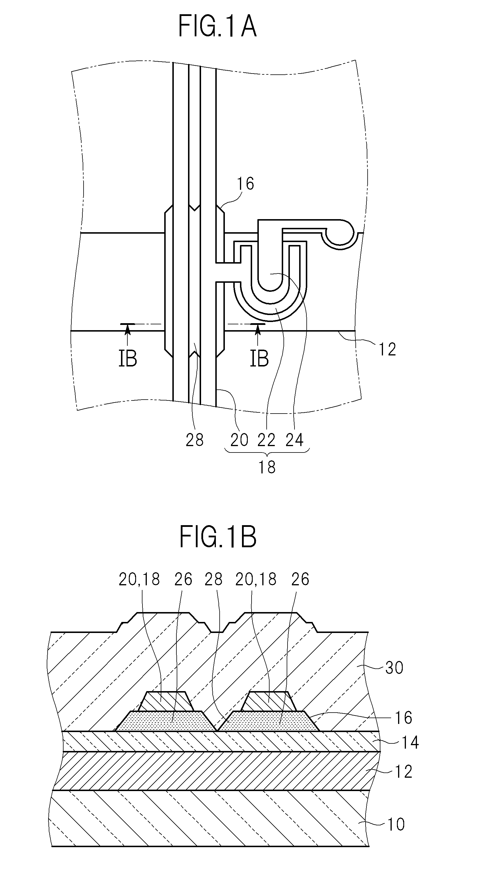
[0046]FIGS. 1A to 4 are views illustrating a manufacturing method for a liquid crystal display device according to a first embodiment of the present invention. FIG. 1B is a cross-sectional view taken along the line IB-IB of a structure illustrated in FIG. 1A. FIG. 2B is a cross-sectional view taken along the line IIB-IIB of a structure illustrated in FIG. 2A. FIG. 3B is a cross-sectional view taken along the line IIIB-IIIB of a structure illustrated in FIG. 3A.
[0047]In this embodiment, as illustrated in FIG. 1B, a first substrate 10 is prepared. The first substrate 10 is formed of a light transmissive material. A gate wiring 12 is formed on the first substrate 10. The gate wiring 12 has a portion which serves as a gate electrode of a thin-film transistor, and is formed of a metal such as copper. The gate wiring 12 may be formed by forming a metal film on an entire surface of the first substrate 10, and then subjecting the metal film to etching. A gate insulating film 14 is formed ab...
second embodiment
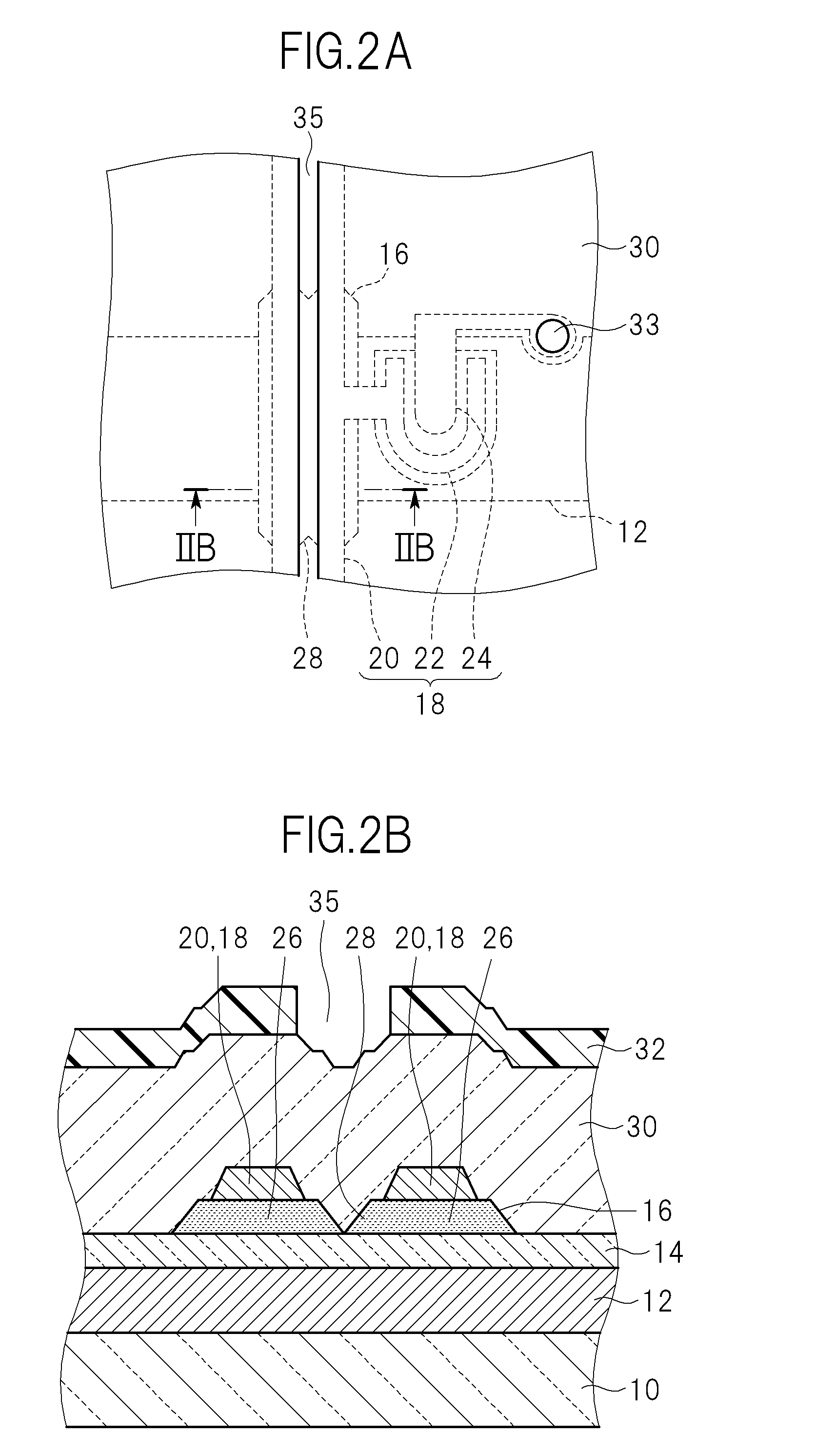
[0064]FIGS. 10A to 12 are views illustrating a manufacturing method for a liquid crystal display device according to a second embodiment of the present invention. FIG. 10B is a cross-sectional view taken along the line XB-XB of a structure illustrated in FIG. 10A. FIG. 11B is a cross-sectional view taken along the line XIB-XIB of a structure illustrated in FIG. 11A.
[0065]In this embodiment, the first substrate 10, the gate wiring 12, and the gate insulating film 14 correspond to those described in the first embodiment.
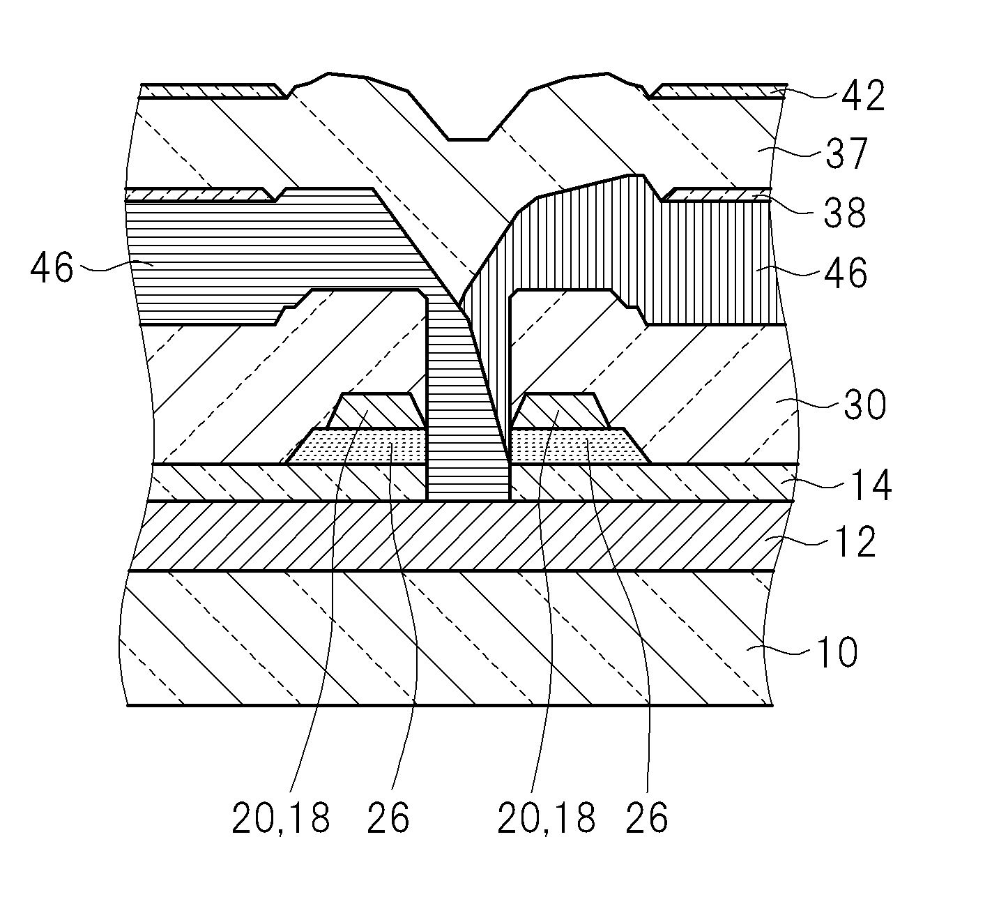
[0066]As illustrated in FIGS. 10A and 10B, a semiconductor pattern 116 and a metal pattern 118 are formed on the gate insulating film 14. Further, in the same layer as the semiconductor pattern 116, the semiconductor layer of the thin-film transistor is formed. The summary of a method of forming the semiconductor pattern and the semiconductor layer is as follows (not shown). The semiconductor film and the metal film are laminated, and the semiconductor film and the met...
third embodiment
[0081]FIG. 18 is a view of a liquid crystal display device according to a third embodiment of the present invention.
[0082]In a manufacturing method for the liquid crystal display device according to this embodiment, steps described in at least one of the first embodiment and the second embodiment are performed. After that, liquid crystal 54 is provided between the first substrate 10 and a second substrate 50 facing the first substrate 10, the liquid crystal 54 being surrounded by a seal portion 52 so as to be sealed.
[0083]The liquid crystal display device in this embodiment includes the first substrate 10 on which thin-film transistors are formed, the second substrate 50 facing the first substrate 10, the liquid crystal 54 provided between the first substrate 10 and the second substrate 50, and the seal portion 52 formed around the liquid crystal 54 between the first substrate 10 and the second substrate 50.
[0084]In the first substrate 10, a semiconductor pattern 216 and a metal pat...
PUM
| Property | Measurement | Unit |
|---|---|---|
| insulating | aaaaa | aaaaa |
| width | aaaaa | aaaaa |
| color | aaaaa | aaaaa |
Abstract
Description
Claims
Application Information
 - R&D
- Intellectual Property
- Life Sciences
- Materials
- Tech Scout
- Unparalleled Data Quality
- Higher Quality Content
- 60% Fewer Hallucinations
Browse by: Latest US Patents, China's latest patents, Technical Efficacy Thesaurus, Application Domain, Technology Topic, Popular Technical Reports.
© 2025 PatSnap. All rights reserved.Legal|Privacy policy|Modern Slavery Act Transparency Statement|Sitemap|About US| Contact US: help@patsnap.com