Joint apparatus

a technology of joint apparatus and connector, which is applied in the direction of metal working apparatus, metal-working machine components, manufacturing tools, etc., can solve the problems of increasing the resistance of the wiring and the increase of the wiring delay, and achieve the effect of suppressing the generation of voids and performing appropriately and efficiently

Active Publication Date: 2014-09-02
TOKYO ELECTRON LTD
View PDF12 Cites 3 Cited by
  • Summary
  • Abstract
  • Description
  • Claims
  • Application Information

AI Technical Summary

Benefits of technology

[0017]According to the present invention, the joint of substrates can be appropriately and efficiently performed while suppressing generation of void between substrates.

Problems solved by technology

When a plurality of highly integrated semiconductor devices are arranged within a horizontal plane and connected with one another by wiring into a product, the wiring length may increase to lead to an increase in resistance of the wiring and increase in a wiring delay.

Method used


Image

  • Joint apparatus
  • Joint apparatus
  • Joint apparatus

Examples


Embodiment Construction

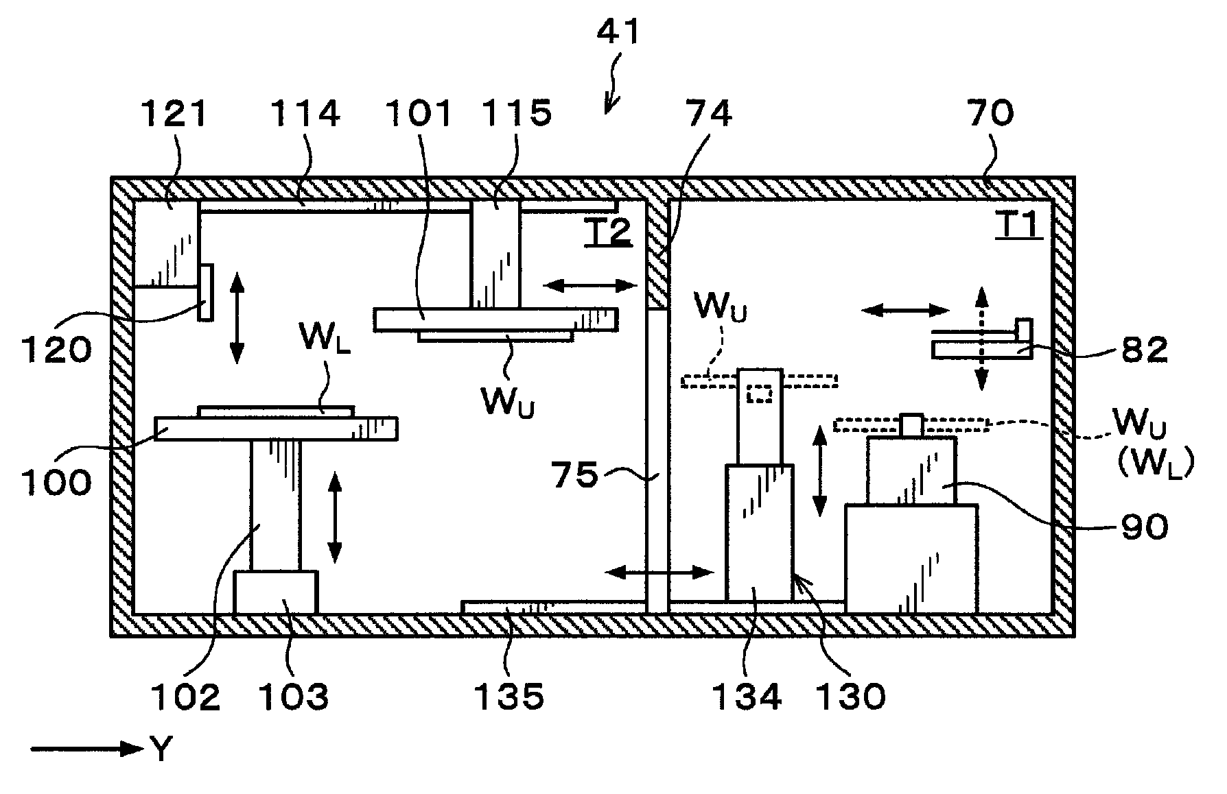
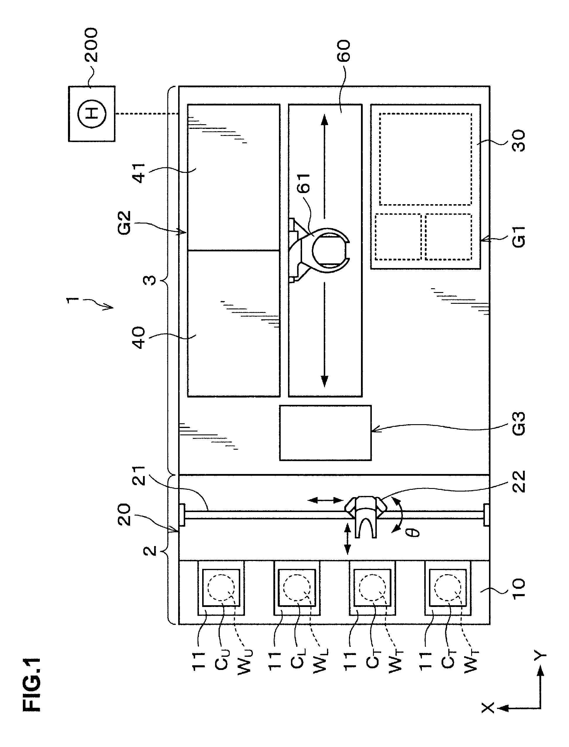
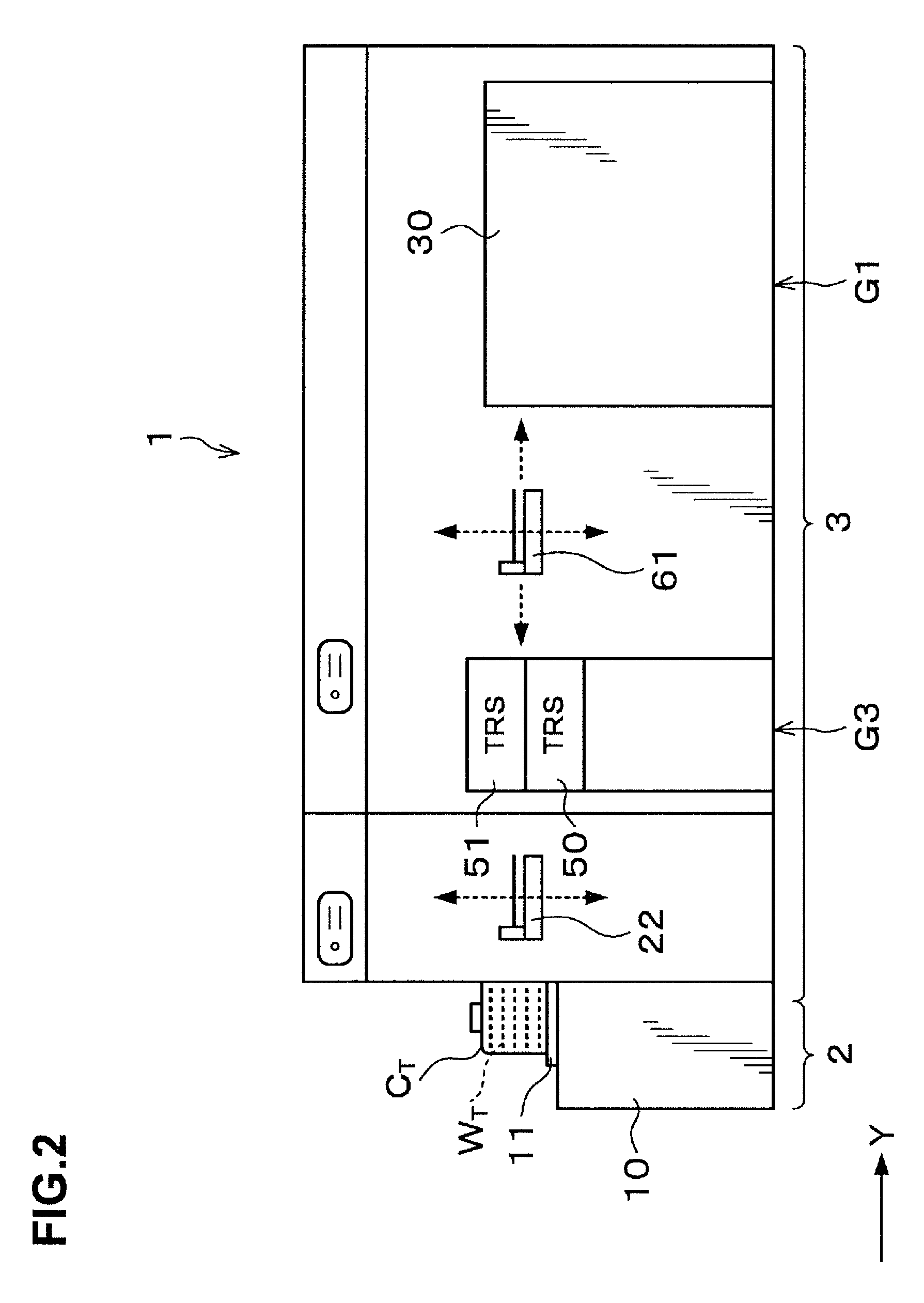
[0036]Hereinafter, an embodiment of the present invention will be described. FIG. 1 is a plan view illustrating the outline of the configuration of a joint system 1 including a joint apparatus according to this embodiment. FIG. 2 is a side view illustrating the outline of the internal configuration of the joint system 1.

[0037]In the joint system 1, for example, wafers WU, WL as two substrates are joined together as illustrated in FIG. 3. Hereinafter, the wafer located on the upper side is referred to as an “upper wafer WU” as a second substrate and the wafer located on the lower side is referred to as a “lower wafer WL” as a first substrate. Further, the joint surface at which the upper wafer WU is to be joined is referred to as a “front surface WU1” and the surface opposite to the front surface WU1 is referred to as a “rear surface WU2.” Similarly, the joint surface at which the lower wafer WL is to be joined is referred to as a “front surface WL1” and the surface opposite to the f...


PUM

PropertyMeasurementUnit
distanceaaaaaaaaaa
temperatureaaaaaaaaaa

Abstract

In a joint apparatus, a transfer region and a processing region are formed. In the transfer region, a transfer mechanism transferring a first substrate, a second substrate, or a superposed substrate, a position adjusting mechanism adjusting an orientation in a horizontal direction of the first substrate or the second substrate, and a reversing mechanism reversing front and rear surfaces of the second substrate are provided. In the processing region, a first holding member mounting and holding the first substrate on an upper surface thereof, a second holding member holding the second substrate on a lower surface thereof, and a pressing and moving member bringing one end portion of the first substrate and one end portion of the second substrate into abutment with each other and pressing the one end portions when joining the first substrate and the second substrate together are provided.

Description

TECHNICAL FIELD[0001]The present invention relates to a joint apparatus joining substrates together.BACKGROUND ART[0002]Recently, semiconductor devices become more highly integrated. When a plurality of highly integrated semiconductor devices are arranged within a horizontal plane and connected with one another by wiring into a product, the wiring length may increase to lead to an increase in resistance of the wiring and increase in a wiring delay.[0003]Hence, it is proposed to use the three-dimensional integration technology of stacking the semiconductor devices in three dimensions. In this three-dimensional integration technology, for example, a bonding apparatus is used to join two semiconductor wafers (hereinafter, referred to as “wafers”). The bonding apparatus has, for example, a chamber housing two wafers arranged one above the other (hereinafter, the wafer on the upper side is referred to as an “upper wafer” and the wafer on the lower side is referred to as a “lower wafer”),...

Claims


Application Information

Patent Timeline
Patent Type & Authority Patents(United States)
IPC IPC(8): B23P21/00B23Q15/00
CPCH01L21/187H01L21/67092Y10T29/5317Y10T29/53096Y10T29/53091H01L27/12H01L21/02
Inventor NISHIBAYASHI, TAKAHIROKITAYAMA, TATSUYAYOSHITAKA, NAOTO
Owner TOKYO ELECTRON LTD
Why Eureka
Try Eureka