Separation of semiconductor devices from a wafer carrier

a technology of semiconductor devices and wafers, applied in the direction of individual semiconductor device testing, semiconductor/solid-state device testing/measurement, instruments, etc., can solve the problem of time-consuming process

Active Publication Date: 2014-11-11
INFINEON TECH AG
View PDF29 Cites 9 Cited by
  • Summary
  • Abstract
  • Description
  • Claims
  • Application Information

AI Technical Summary

Benefits of technology

[0004]These and other problems are generally solved or circumvented, and technical advantages are generally achieved, by illustrative embodiments of the present invention.

Problems solved by technology

However, such a process is time consuming and may become the bottleneck for the overall production.

Method used


Image

  • Separation of semiconductor devices from a wafer carrier
  • Separation of semiconductor devices from a wafer carrier
  • Separation of semiconductor devices from a wafer carrier

Examples


Embodiment Construction

[0018]The making and using of various embodiments are discussed in detail below. It should be appreciated, however, that the present invention provides many applicable inventive concepts that can be embodied in a wide variety of specific contexts. The specific embodiments discussed are merely illustrative of specific ways to make and use the invention, and do not limit the scope of the invention.

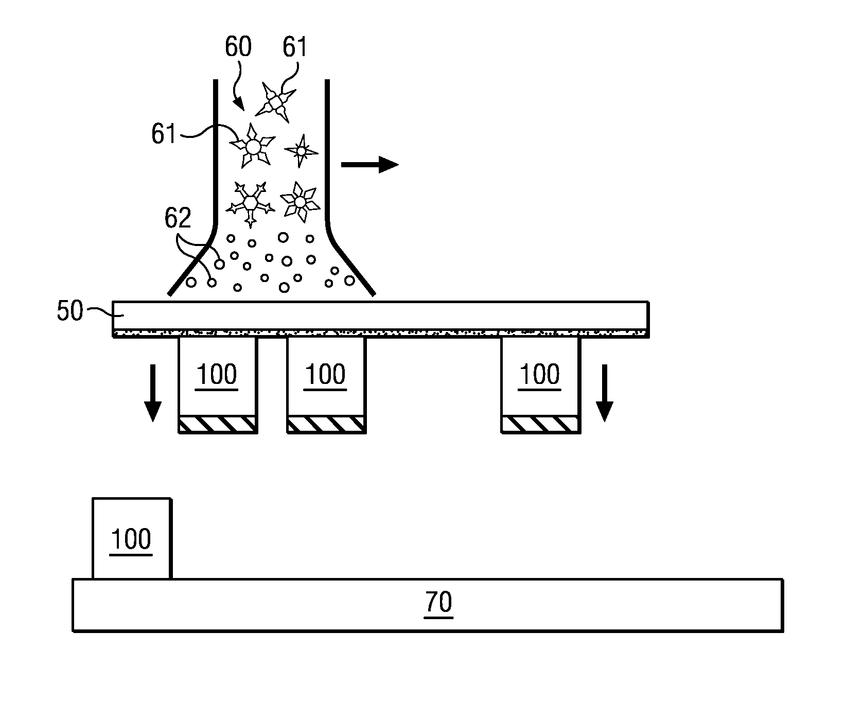
[0019]A method for rapidly removing semiconductor dies attached to a wafer frame (a frame with an adhesive foil) or carrier will be described using FIGS. 1-10, 17-18, 19-21 in accordance with embodiments of the invention. A carbon dioxide snow jet as used by embodiments of the invention will be described using FIG. 11. An embodiment for removing, e.g., defective dies from a frame with an adhesive foil will be described using FIG. 12. An embodiment of the invention will be described for removal of packaged semiconductor dies will be described using FIG. 13-16.

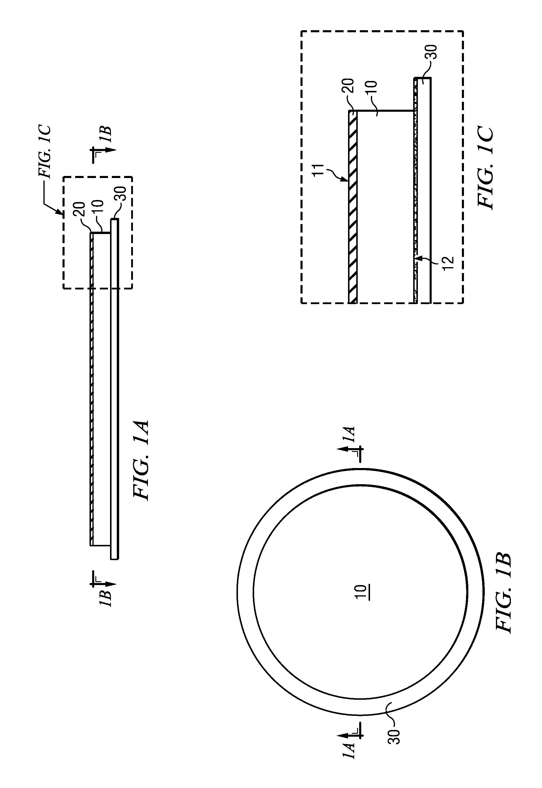
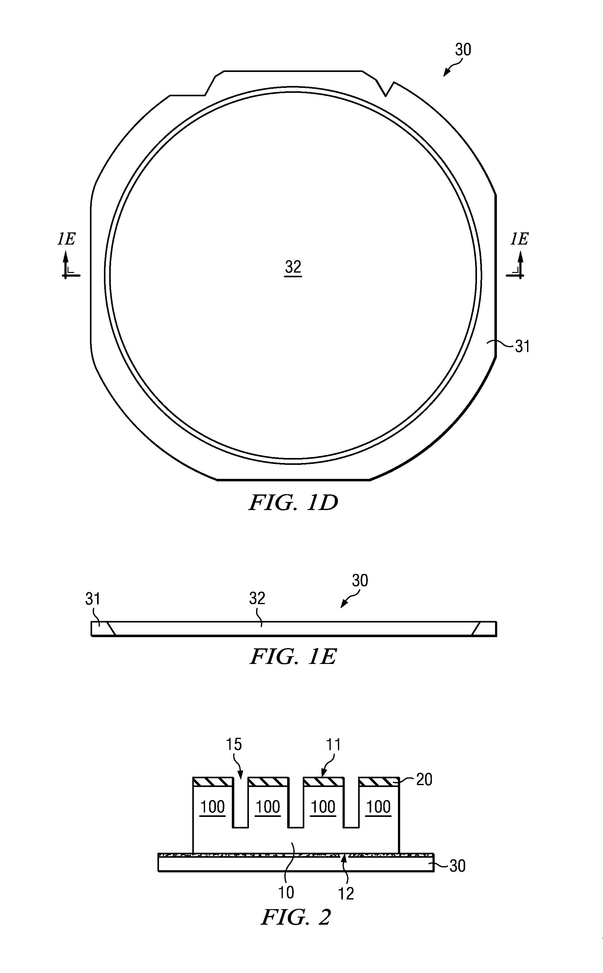
[0020]FIGS. 1-11 illustrates a me...


PUM


Abstract

In accordance with an embodiment of the present invention, a semiconductor device is manufactured by arranging a plurality of semiconductor devices on a frame with an adhesive foil. The plurality of semiconductor devices is attached to the adhesive foil. The plurality of semiconductor devices is removed from the frame with the adhesive foil using a carbon dioxide snow jet and / or a laser process.

Description

TECHNICAL FIELD[0001]The present invention relates generally to a method, and more particularly to a method for separation of semiconductor devices from a wafer carrier.BACKGROUND[0002]Semiconductor devices are used in many electronic and other applications. Semiconductor devices may comprise integrated circuits that are formed on semiconductor wafers. Alternatively, semiconductor devices may be formed as monolithic devices, e.g., discrete devices. Semiconductor devices are formed on semiconductor wafers by depositing many types of thin films of material over the semiconductor wafers, patterning the thin films of material, doping selective regions of the semiconductor wafers, etc.[0003]In a conventional semiconductor fabrication process, a large number of semiconductor devices are fabricated in a single wafer. After completion of device level and interconnect level fabrication processes, the semiconductor devices on the wafer are separated. For example, the wafer may undergo singula...

Claims


Application Information

Patent Timeline
Patent Type & Authority Patents(United States)
IPC IPC(8): H01L21/56H01L21/78H01L21/683H01L21/00H01L21/50H01L21/67H01L23/31
CPCH01L21/561H01L21/50H01L21/683H01L2924/00H01L21/78H01L21/67H01L2924/0002H01L21/565H01L21/568H01L23/3107H01L2221/68327H01L2221/68381H01L2221/68322H01L2221/6834H01L21/67144H01L21/6836H01L2221/68368H01L21/67092
Inventor VAUPEL, MATHIASBERNRIEDER, SEBASTIANKOLLER, ADOLFMARTENS, STEFAN
Owner INFINEON TECH AG
Why Eureka
Try Eureka