Array antenna apparatus having shortest wiring distance to antenna elements

a technology of antenna elements and antenna antennas, applied in the field of array antenna apparatuses, can solve the problems of low noise performance, insufficient output power covered by antenna directional gain, and difficult to obtain high directional gain by a single element, so as to reduce the area and loss of relevant radio apparatus, reduce the redundancy of the feeder line

Active Publication Date: 2014-11-18
NEC CORP
View PDF14 Cites 0 Cited by
  • Summary
  • Abstract
  • Description
  • Claims
  • Application Information

AI Technical Summary

Benefits of technology

[0056]In accordance with the present invention, it is possible that a delay circuit is provided at a feeder line which connects a radio circuit and each antenna element and the delay amount thereof is set so that the sum of a phase delay by the delay circuit and a phase delay due to a difference between the length of the feeder line and a reference length is an integer multiple of 360 degrees. Accordingly, (i) the redundancy of the feeder line can be reduced so that the area and loss of the relevant radio apparatus can be reduced, and (ii) the input phases for the antennas can be equalized.

Problems solved by technology

Since transmission (reception) amplifiers for high-frequency bands are required to have a small (electric) power amplifying gain and a low power consumption, it is difficult to obtain high output power (i.e., low noise performance).
Therefore, insufficient output power is covered using directional gain of an antenna.
Generally, planar antennas have a minute open area, and thus it is difficult to obtain a high directional gain by a single element.
This is because if phase and power with respect to the input into the antenna elements are irregular, the beam emitted from the array antenna is not perpendicular to the relevant antenna plane, which also causes an increase in the level of side lobes.
However, in the high-frequency bands such as milliwave bands, the equal-length wiring may degrade the performance of radio apparatuses as described below.
In this case, in order to feed an antenna element close to the signal source, line arrangement for excess length is performed, which requires an extra useless space.
In addition, the larger the number of the antenna elements, the harder the arrangement thereof becomes.

Method used


Image

  • Array antenna apparatus having shortest wiring distance to antenna elements
  • Array antenna apparatus having shortest wiring distance to antenna elements
  • Array antenna apparatus having shortest wiring distance to antenna elements

Examples


first embodiment

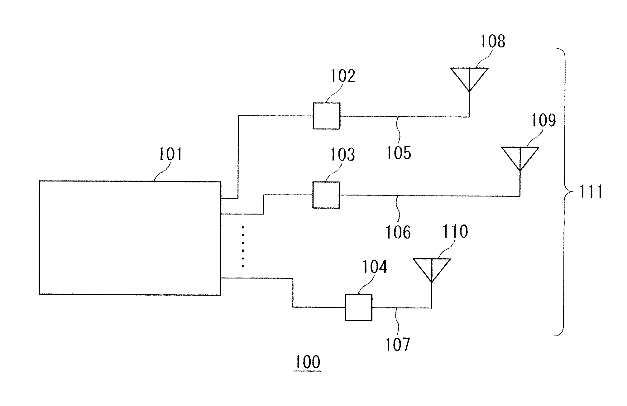
[0072]FIG. 1 is a block diagram showing the structure of an array antenna apparatus as the present invention. In FIG. 1, an array antenna apparatus 100 consists of a radio circuit 101, an array antenna 111, feeder lines 105, 106, and 107, and delay circuits 102, 103, and 104. The array antenna 111 consists of antenna elements 108, 109, and 110.

[0073]A high-frequency signal output from the radio circuit 101 is supplied to the antenna elements 108, 109, and 110 via the corresponding feeder lines 105, 106, and 107. The delay circuits 102, 103, and 104 are inserted in the middle of the corresponding feeder lines 105, 106, and 107 so as to adjust the input phases for the antenna elements 108, 109, and 110.

[0074]The feeder lines 105, 106, and 107 each have any length.

[0075]The amount of phase delay provided by each of the delay circuits 102, 103, and 104 is defined so that the sum of the phase delay by the relevant delay circuit and a phase delay due to a difference between a reference le...

second embodiment

[0087]FIG. 4 is a block diagram showing the structure of an array antenna apparatus as the present invention. In an array antenna apparatus 400 of FIG. 4, delay circuits 402, 403, and 404 are provided in the radio circuit 101 of the array antenna apparatus 100 of FIG. 1, while the delay circuits 102, 103, and 104 are omitted. In other words, the delay circuits 402, 403, and 404 are provided at the feeder lines 105, 106, and 107 within the radio circuit 101.

[0088]According to the above structure, effects similar to the first embodiment can be obtained, and complexity in the wiring caused by providing the delay circuits at the feeder lines can be reduced.

[0089]That is, since the delay circuits are provided in the radio circuit, an area to be occupied by the delay circuits can be omitted in the feeder line area. Therefore, no detour for avoiding the delay circuits is necessary, thereby reducing the complexity in the wiring.

third embodiment

[0090]FIG. 5 is a block diagram showing the structure of an array antenna apparatus as the present invention. In an array antenna apparatus 500 of FIG. 5, mixer circuits 519, 520, and 521 are respectively connected to the feeder lines 105, 106, and 107 which are connected to the antenna elements 108, 109, and 110 which form the array antenna 111. To the mixer circuits 519, 520, and 521, local signal lines 513, 514, and 515 and base band signal lines 516, 517, and 518 are respectively connected. In addition, delay circuits 402, 403, and 405 are respectively provided at the base band signal lines 516, 517, and 518.

[0091]The mixer circuits 519, 520, and 521 and the delay circuits 402, 403, and 405 are arranged in the radio circuit 101.

[0092]In comparison with the array antenna apparatus 400 of FIG. 4, the array antenna apparatus 500 has a structure in which the delay circuits are provided at the base band signal limes. The delay circuits 402, 403, and 405 control the phases of base ban...


PUM


Abstract

An array antenna apparatus includes a radio circuit; an array antenna that includes a plurality of antenna elements; feeder lines that connect the radio circuit to the respective antenna elements; and a delay circuit provided at each of one or more of the feeder lines. An amount of delay of the delay circuit is set so that the sum of a phase delay by the delay circuit and a phase delay due to a difference between a length of the corresponding feeder line and a predetermined reference length is an integer multiple of 360 degrees.

Description

TECHNICAL FIELD[0001]The present invention relates to an array antenna apparatus which has an array antenna, a feeder line, and a radio circuit.[0002]Priority is claimed on Japanese Patent Application No. 2009-289139, filed Dec. 21, 2009, the contents of which are incorporated herein by reference.BACKGROUND ART[0003]In recent years, demand for Gbps-level high speed data communication has been improved for indoor radio apparatuses. In such Gbps-level high speed data communication, usage of high-frequency bands such as 60 GHz bands (i.e., milliwave bands) has been advanced.[0004]Since transmission (reception) amplifiers for high-frequency bands are required to have a small (electric) power amplifying gain and a low power consumption, it is difficult to obtain high output power (i.e., low noise performance). Therefore, insufficient output power is covered using directional gain of an antenna.[0005]For indoor use of a radio apparatus, downsizing of the relevant communication module is r...

Claims


Application Information

Patent Timeline
Patent Type & Authority Patents(United States)
IPC IPC(8): H01Q3/30H01Q21/00H01Q21/06H04B7/06
CPCH01Q21/061H04B7/0671H01Q3/30
Inventor ORIHASHI, NAOYUKI
Owner NEC CORP
Why Eureka
Try Eureka